Meta patents chip design that disables unused parts of a processor
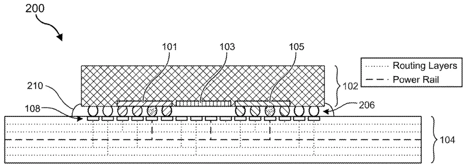
Meta describes a chip packaging method where two different circuits are placed on the same silicon die. The design connects the first circuit to the outside pins while leaving the second circuit disconnected, effectively turning it off.
In the filing’s own words
Apparatuses include a package substrate with package bonding pads and a die electrically coupled to the package substrate via conductive bonding elements. The die includes a first application-specific integrated circuit (ASIC) with first die input/output pads and a second ASIC with second die input/output pads. Each of the first die input/output pads is electrically coupled to at least one corresponding package bonding pad. At least one of the second die input/output pads is not electrically coupled to any package bonding pad, such that the second ASIC is left in an inoperable state.
What exactly they claim (claim 1)
1. An apparatus, comprising: a package substrate comprising a plurality of package bonding pads; and a die electrically coupled to the package substrate via a plurality of conductive bonding elements, wherein: the die comprises: a first application-specific integrated circuit comprising first die input/output pads; and a second application-specific integrated circuit comprising second die input/output pads; each of the first die input/output pads of the first application-specific integrated circuit is electrically coupled to at least one corresponding package bonding pad of the package substrate by at least one of the plurality of conductive bonding elements; and at least one of the second die input/output pads of the second application-specific integrated circuit is not electrically coupled to any package bonding pad of the package substrate such that the second application-specific integrated circuit is left in an inoperable state.
Facts
- Company
- Meta (Meta Platforms Technologies, LLC)
- Official title
- Universal chip with variable packaging
- Patent number
- US12805357B2
- Application number
- 18534143
- Filed
- Dec 8, 2023
- Granted
- Nov 17, 2026
- Inventors
- 1
- Claims
- 20
Classified under
H10W 70/65 Electricity & electronicsH10W 90/00 Electricity & electronicsH10W 90/724 Electricity & electronicsH10W 90/725 Electricity & electronicsH10W 90/794 Electricity & electronicsMore from Meta in Chips & hardware
- Meta patents flexible diamond layer to cool computer chips Sep 17, 2026
- Meta patents plastic chip connector that also spreads heat Sep 15, 2026
- Meta patents OLED screens with crystals that control light direction Nov 17, 2026
- Meta patents handheld device that mimics controller inputs using motion sensors Sep 24, 2026
- Meta patents display tech that stacks processors under screen pixels Oct 22, 2026
Summaries are simplified from the filing’s own abstract and first claim. A patent filing is not a product announcement.
Patent data and drawings: U.S. Patent and Trademark Office (USPTO). Nebula is not affiliated with or endorsed by the USPTO.