Sony patents chip design with separate top and bottom electrical paths
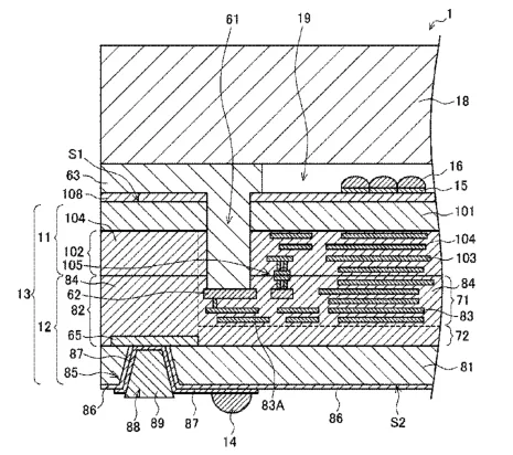
Sony describes a semiconductor device where a metal pad sits at the bottom of a hole filled with insulating material on the chip's surface. A wiring layer connects this pad to a separate through-electrode that passes through the chip from the opposite side, keeping the two connection points in different areas of the chip.
In the filing’s own words
Provided is a semiconductor device including a stack including a semiconductor substrate, an opening provided extending from a first surface of the stack and filled with an insulating material, a pad electrode provided at a bottom of the opening, a wiring layer provided in a planar region of the stack overlapping a planar region where the opening is provided in plan view from the first surface, the wiring layer being electrically being connected to the pad electrode, and a through electrode provided in a planar region different from the planar region where the opening is provided in the plan view and provided extending from a second surface of the stack opposite to the first surface.
What exactly they claim (claim 1)
1. A semiconductor device, comprising: a stack including a semiconductor substrate; an opening extending from a first surface of the stack and filled with an insulating material; a pad electrode disposed at a bottom of the opening; a wiring layer disposed in a first planar region of the stack that overlaps, in a plan view from the first surface, a second planar region where the opening is located, the wiring layer being electrically connected to the pad electrode; and a through electrode disposed in a third planar region that is laterally spaced from and does not overlap the second planar region in the plan view, the through electrode extending from a second surface of the stack opposite to the first surface.
Facts
- Company
- Sony (SONY SEMICONDUCTOR SOLUTIONS CORPORATION)
- Official title
- Semiconductor device
- Patent number
- US12805269B2
- Application number
- 18551251
- Filed
- Jan 13, 2022
- Granted
- Nov 17, 2026
- Inventors
- 2
- Claims
- 20
Classified under
H10P 74/273 Electricity & electronicsH10F 39/026 Electricity & electronicsH10F 39/804 Electricity & electronicsH10F 39/809 Electricity & electronicsH10F 39/811 Electricity & electronicsMore from Sony in Chips & hardware
- Sony patents stacked image sensor with built-in AI processing Nov 17, 2026
- Sony patents light sensor that adjusts how it counts incoming photons Sep 1, 2026
- Sony patents camera sensor with two pixel types for better motion detection Sep 1, 2026
- Sony patents game graphics that adjust quality based on hardware heat Sep 8, 2026
- Sony patents camera sensor design that stacks chips to shrink pixels Sep 8, 2026
Summaries are simplified from the filing’s own abstract and first claim. A patent filing is not a product announcement.
Patent data and drawings: U.S. Patent and Trademark Office (USPTO). Nebula is not affiliated with or endorsed by the USPTO.