Sony patents stacked image sensor with built-in AI processing
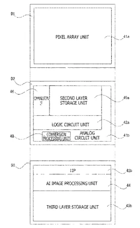
Sony describes an image sensor made of three stacked layers to save space. The bottom layer captures light, the middle layer converts it to digital data, and the top layer runs AI calculations directly on that data. This design places the processing circuits next to the conversion circuits rather than on top of them.
In the filing’s own words
An image sensor according to the present technology has a layered structure that includes a first layer, a second layer, and a third layer. The first layer includes a pixel array unit where multiple pixels are two-dimensionally arrayed. The second layer includes a conversion processing unit configured to perform A/D conversion for converting an analog signal based on a pixel signal output from the pixel array unit, into a digital signal, and a second layer storage unit configured to store image data for each frame, the image data being digital data based on the digital signal. The third layer includes an inference processing unit configured to perform an inference process on the basis of the image data as an input tensor.
What exactly they claim (claim 1)
1. An image sensor comprising: a layered structure that includes a first layer that includes a pixel array where multiple pixels are two-dimensionally arrayed, a second layer that includes conversion processing circuitry configured to perform A/D conversion for converting an analog signal based on a pixel signal output from the pixel array, into a digital signal, and a second layer memory configured to store image data for each frame, the image data being digital data based on the digital signal, and a third layer that includes inference processing circuitry configured to perform an inference process based on the image data as an input tensor, wherein the conversion processing circuitry and the inference processing circuitry are disposed at positions not overlapping each other in a lamination direction of the respective layers.
Facts
- Company
- Sony (Sony Semiconductor Solutions Corporation)
- Official title
- Image sensor with layered structure for size reduction
- Patent number
- US12804288B2
- Application number
- 18855654
- Filed
- Apr 24, 2023
- Granted
- Nov 17, 2026
- Inventors
- 1
- Claims
- 11
Classified under
H04N 25/772 Electricity & electronicsH10F 39/802 Electricity & electronicsH10F 39/803 Electricity & electronicsMore from Sony in Chips & hardware
- Sony patents light sensor that adjusts how it counts incoming photons Sep 1, 2026
- Sony patents camera sensor with two pixel types for better motion detection Sep 1, 2026
- Sony patents game graphics that adjust quality based on hardware heat Sep 8, 2026
- Sony patents camera sensor design that stacks chips to shrink pixels Sep 8, 2026
- Sony patents chip design that measures internal temperature from outside Sep 8, 2026
Summaries are simplified from the filing’s own abstract and first claim. A patent filing is not a product announcement.
Patent data and drawings: U.S. Patent and Trademark Office (USPTO). Nebula is not affiliated with or endorsed by the USPTO.