Microsoft patents superconductor chip design with dual-layer control gates
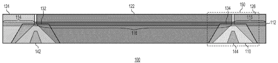
Microsoft describes a topological superconductor device that uses a wire patterned on a 2D electron gas. The design features two distinct layers of control gates: "plunger" gates that tune the wire's properties and "cutter" gates that open or close junctions at the wire's ends.
In the filing’s own words
Topological superconductor devices with gates formed in two gate layers are described. A topological superconductor device includes a superconducting wire having a first junction near a first end of the superconducting wire and a second junction near a second end, opposite to the first end. The topological superconductor device further includes: (1) a first side-plunger gate and a second-side plunger gate formed in a first gate layer of the topological superconductor device, (2) a middle-plunger gate formed in the first gate layer of the topological superconductor device, (3) a first cutter gate formed in a second layer, different from the first layer, of the topological superconductor device, and (4) a second cutter gate formed in the second layer of the topological superconductor device. The plunger gates are operable to tune respective sections of the superconducting wire and the cutter gates are operable to open and close the respective junctions.
What exactly they claim (claim 1)
1. A topological superconductor device comprising: a superconducting wire having a first junction near a first end of the superconducting wire and a second junction near a second end, opposite to the first end, of the superconducting wire, wherein the superconducting wire is patterned on a two-dimensional electron gas (2DEG); a first dielectric layer formed over the superconducting wire; a first side-plunger gate formed in a first layer, above the first dielectric layer, of the topological superconductor device, wherein the first side-plunger gate is operable to tune a first section of the superconducting wire located between the first junction and the first end of the superconducting wire; a second side-plunger gate formed in the first layer of the topological superconductor device, wherein the second side-plunger gate is operable to tune a second section of the superconducting wire located between the second junction and the second end of the superconducting wire; a middle-plunger gate formed in the first layer of the topological superconductor device, wherein the middle-plunger gate is operable to tune a middle section of the superconducting wire located between the first junction and the second junction; a first helper gate formed in the first layer of the topological superconductor device, wherein the first helper gate is operable to control a density of electrons in a first region of the 2DEG; and a second helper gate formed in the first layer of the topological superconductor device, wherein the second helper gate is operable to control a density of electrons in a second region, different from the first region, of the 2DEG; a second dielectric layer formed over each of the first side-plunger gate, the second side-plunger gate, the middle-plunger gate, the first helper gate, and the second helper gate; a first cutter gate formed in a second layer, above the second dielectric layer, of the topological superconductor device, wherein the first cutter gate is operable to open and close the first junction; and a second cutter gate formed in the second layer of the topological superconductor device, wherein the second cutter gate is operable to open and close the second junction.
Facts
- Company
- Microsoft (Microsoft Technology Licensing, LLC)
- Official title
- Topological superconductor devices with two gate layers
- Patent number
- US12805203B2
- Application number
- 17980886
- Filed
- Nov 4, 2022
- Granted
- Nov 17, 2026
- Inventors
- 6
- Claims
- 20
Classified under
H10N 60/128 Electricity & electronicsH10N 60/0884 Electricity & electronicsMore from Microsoft in Chips & hardware
- Microsoft patents DNA builder that adds bases in a chosen order Nov 10, 2026
- Microsoft patents chips with liquid cooling built inside Oct 1, 2026
- Microsoft patents light-based math for faster computing Oct 29, 2026
- Microsoft patents chip design that guesses code steps ahead Sep 8, 2026
- Microsoft patents 3D glass storage using laser light patterns Sep 8, 2026
Summaries are simplified from the filing’s own abstract and first claim. A patent filing is not a product announcement.
Patent data and drawings: U.S. Patent and Trademark Office (USPTO). Nebula is not affiliated with or endorsed by the USPTO.