Sony patents stacked camera sensor design with improved connections
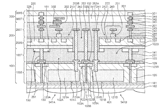
Sony describes a camera sensor made by stacking two layers of silicon chips to improve how they connect. The design uses small holes and a specific groove structure to link the light-capturing layer with the circuit layer behind it.
In the filing’s own words
In an imaging element obtained by stacking a plurality of semiconductor substrates, connection between semiconductor substrates is facilitated. The imaging element includes a first semiconductor substrate, a second semiconductor substrate, an insulating layer, connection sections, and a recess. The first semiconductor substrate includes photoelectric conversion sections that perform photoelectric conversion of incident light. The second semiconductor substrate includes pixel circuits that generate an image signal corresponding to a charge generated by the photoelectric conversion, and the first semiconductor substrate is stacked on the back side of the second semiconductor substrate. The insulating layer is disposed between the first semiconductor substrate and the second semiconductor substrate. A connection section penetrates through the insulating layer and connects the first semiconductor substrate and the back side of the second semiconductor substrate. The recess is disposed on a surface of the insulating layer adjacent to the second semiconductor substrate and is formed around the connection sections.
What exactly they claim (claim 1)
1. An imaging element, comprising: a first semiconductor substrate including a photoelectric conversion section configured to perform photoelectric conversion of incident light to generate a charge; a second semiconductor substrate including a pixel circuit configured to generate an image signal corresponding to the charge generated by the photoelectric conversion, the second semiconductor substrate stacked with the first semiconductor substrate on a back side of the second semiconductor substrate; an insulating layer between the first semiconductor substrate and the second semiconductor substrate; a connection section penetrating through the insulating layer and connecting the first semiconductor substrate and the back side of the second semiconductor substrate, wherein the second semiconductor substrate further includes a first semiconductor region connected to the connection section, and the first semiconductor region has a higher impurity concentration than that of a region of the second semiconductor substrate; and a recess on a surface of the insulating layer, wherein the surface of the insulating layer is adjacent to the second semiconductor substrate, and the recess is around the connection section.
Facts
- Company
- Sony (SONY SEMICONDUCTOR SOLUTIONS CORPORATION)
- Official title
- Imaging element and imaging device
- Patent number
- US12805049B2
- Application number
- 18550693
- Filed
- Feb 28, 2022
- Granted
- Nov 17, 2026
- Inventors
- 2
- Claims
- 16
Classified under
H10F 39/811 Electricity & electronicsH10F 39/18 Electricity & electronicsH10F 39/809 Electricity & electronicsMore from Sony in Chips & hardware
- Sony patents stacked image sensor with built-in AI processing Nov 17, 2026
- Sony patents light sensor that adjusts how it counts incoming photons Sep 1, 2026
- Sony patents camera sensor with two pixel types for better motion detection Sep 1, 2026
- Sony patents game graphics that adjust quality based on hardware heat Sep 8, 2026
- Sony patents camera sensor design that stacks chips to shrink pixels Sep 8, 2026
Summaries are simplified from the filing’s own abstract and first claim. A patent filing is not a product announcement.
Patent data and drawings: U.S. Patent and Trademark Office (USPTO). Nebula is not affiliated with or endorsed by the USPTO.