Google patents display tech that shrinks pixels for mobile screens
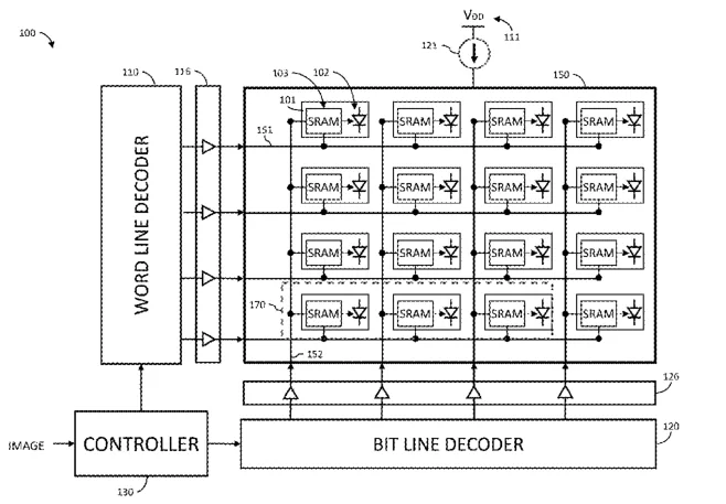
Google has been granted a patent for a display design that packs color pixels closer together to fit high-resolution screens into small devices. The invention uses a shared electrical structure for the control components of each pixel, allowing the physical size of the pixel group to shrink significantly. This layout aims to reduce power usage by matching the voltage supply to the specific needs of the light-emitting components.
In the filing’s own words
A high-resolution display that is a small size suitable for mobile applications is disclosed. The display is color and so includes different color subpixels arranged in subpixel groups. To minimize power consumption, each subpixel includes its own power rail supplying the subpixel with a rail voltage that is based on a forward voltage of a corresponding light emitting diode. To minimize the area of the subpixel group, transistors of the subpixels are fabricated within a common well and the body terminals of the transistors are connected to a common well rail that is separate from the power rails.
What exactly they claim (claim 1)
1. A subpixel group for a display comprising: a plurality of power rails configured to supply rail voltages to a plurality of light emitting diodes; a plurality of drive transistors fabricated within a single common well in a substrate, the common well configured to enable a pitch between the plurality of light emitting diodes of less than five microns, each drive transistor coupled in series between a power rail and a respective light emitting diode; a plurality of memory cells coupled to respective terminals of the plurality of drive transistors to control the plurality of light emitting diodes; and a well rail coupled to a body terminal of each drive transistor, the well rail configured to supply a single bulk voltage to the single common well via the body terminal of each drive transistor, the single bulk voltage being greater than any of the rail voltages supplied by the plurality of power rails to prevent forward biasing of body diodes formed between the plurality of drive transistors and the single common well.
Facts
- Company
- Google (GOOGLE LLC)
- Official title
- Multi-rail subpixel group for a display
- Patent number
- US12802618B2
- Application number
- 18932204
- Filed
- Oct 30, 2024
- Granted
- Nov 17, 2026
- Inventors
- 2
- Claims
- 18
Classified under
G09G 3/32 Physics & computingH10W 90/00 Electricity & electronicsG09G 2300/0426 Physics & computingG09G 2300/0842 Physics & computingG09G 2330/028 Physics & computingMore from Google in Chips & hardware
- Google patents radar network to track users across multiple devices Nov 10, 2026
- Google patents quantum gates to simulate particle physics Sep 1, 2026
- Waymo patents lidar chips that split light into multiple beams Sep 8, 2026
- Google patents chip design to speed up AI math tasks Sep 8, 2026
- Google patents display that turns off colors to save battery Sep 8, 2026
Summaries are simplified from the filing’s own abstract and first claim. A patent filing is not a product announcement.
Patent data and drawings: U.S. Patent and Trademark Office (USPTO). Nebula is not affiliated with or endorsed by the USPTO.