Samsung patents chip design that splits math tasks to speed up AI processing
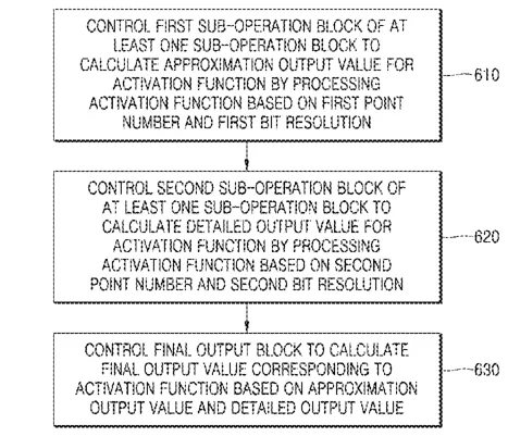
Samsung has been granted a patent for a specific hardware design inside a neural processing unit (NPU), which is a chip part dedicated to running AI models. The design uses an accelerator that splits the calculation of an activation function into two parts: a quick, rough estimate and a more precise, detailed calculation. A final block then combines these two results to produce the final output, aiming to handle complex math more efficiently.
In the filing’s own words
An electronic device includes: a neural processing unit (NPU) configured to process an activation function; and an accelerator in the NPU, wherein the accelerator includes: a function processing block including at least one sub-operation block, and a final output block connected to the function processing block, wherein the at least one sub-operation block includes: a first sub-operation block configured to calculate an approximation output value for the activation function by processing the activation function based on a first point number and a first bit resolution, and a second sub-operation block configured to calculate a detailed output value for the activation function by processing the activation function based on a second point number and a second bit resolution, and wherein the final output block is configured to calculate a final output value corresponding to the activation function based on the approximation output value and the detailed output value.
What exactly they claim (claim 1)
1. An electronic device comprising: a neural processing unit (NPU) configured to process an activation function; and an accelerator in the NPU, wherein the accelerator comprises: a function processing block comprising at least one sub-operation block, and a final output block connected to the function processing block, wherein the at least one sub-operation block comprises: a first sub-operation block configured to calculate an approximation output value for the activation function by processing the activation function based on a first point number and a first bit resolution, and a second sub-operation block configured to calculate a detailed output value for the activation function by processing the activation function based on a second point number and a second bit resolution, and wherein the final output block is configured to calculate a final output value corresponding to the activation function based on the approximation output value and the detailed output value.
Facts
- Company
- Samsung (SAMSUNG ELECTRONICS CO., LTD.)
- Official title
- Electronic device including accelerator for processing function and method of controlling the electronic device
- Patent number
- US12801904B2
- Application number
- 18647814
- Filed
- Apr 26, 2024
- Granted
- Nov 17, 2026
- Inventors
- 3
- Claims
- 20
Classified under
G06N 3/048 Physics & computingG06N 3/063 Physics & computingMore from Samsung in Chips & hardware
- Samsung patents quantum chip design using tiny electron traps Nov 12, 2026
- Samsung patents chip that combines camera and screen Oct 13, 2026
- Samsung patents chip that hides encrypted data from the main processor Oct 27, 2026
- Samsung patents display with tiny holes to hide cameras behind the screen Nov 3, 2026
- Samsung patents faster chip testing using machine learning Sep 1, 2026
Summaries are simplified from the filing’s own abstract and first claim. A patent filing is not a product announcement.
Patent data and drawings: U.S. Patent and Trademark Office (USPTO). Nebula is not affiliated with or endorsed by the USPTO.