Samsung patents display with tiny holes to hide cameras behind the screen
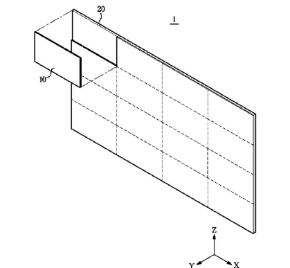
This filing describes a display module where the screen itself contains specific transparent areas. These areas are made of tiny pinholes in the power layers, allowing light to pass through to an image sensor located behind the panel.
In the filing’s own words
A display module includes: a plurality of pixels arranged in two dimensions; a display panel including: a back plate including: a transparent substrate; a pixel circuit layer; and a plurality of power electrode layers provided on the transparent substrate; and a plurality of inorganic light emitting elements provided on the back plate; and an image sensor provided on the rear of the display panel, wherein each of the plurality of pixels includes two or more inorganic light emitting elements among the plurality of inorganic light emitting elements, the display panel includes a plurality of transparent regions in a region corresponding to a position of the image sensor, and each transparent region of the plurality of transparent regions is configured to allow external light to be incident on the image sensor.
What exactly they claim (claim 1)
1. A display module comprising: a plurality of pixels arranged in two dimensions; a display panel comprising: a back plate comprising: a transparent substrate; a pixel circuit layer; and a plurality of power electrode layers provided on the transparent substrate; and a plurality of inorganic light emitting elements provided on the back plate; and an image sensor provided on the rear of the display panel, wherein each of the plurality of pixels comprises two or more inorganic light emitting elements among the plurality of inorganic light emitting elements, wherein the display panel comprises a plurality of transparent regions in a region corresponding to a position of the image sensor, and each transparent region of the plurality of transparent regions is configured to allow external light to be incident on the image sensor, wherein each transparent region of the plurality of transparent regions is provided between apertures of two or more pixels among the plurality of pixels, and wherein each transparent region of the plurality of transparent regions comprises a plurality of pinholes respectively provided in the plurality of power electrode layers and overlapping in a stacking direction of the plurality of power electrode layers.
Facts
- Company
- Samsung (SAMSUNG ELECTRONICS CO., LTD.)
- Official title
- Display module, display apparatus and method for manufacturing same
- Patent number
- US12787437B2
- Application number
- 18227162
- Filed
- Jul 27, 2023
- Granted
- Nov 3, 2026
- Inventors
- 2
- Claims
- 15
Classified under
H10D 86/60 Electricity & electronicsH10D 86/441 Electricity & electronicsH10D 86/451 Electricity & electronicsH10H 20/855 Electricity & electronicsH10W 90/00 Electricity & electronicsH10W 72/90 Electricity & electronicsMore from Samsung in Chips & hardware
- Samsung patents quantum chip design using tiny electron traps Nov 12, 2026
- Samsung patents chip that combines camera and screen Oct 13, 2026
- Samsung patents chip that hides encrypted data from the main processor Oct 27, 2026
- Samsung patents faster chip testing using machine learning Sep 1, 2026
- Samsung patents radar method to pinpoint target direction more accurately Sep 1, 2026
Summaries are simplified from the filing’s own abstract and first claim. A patent filing is not a product announcement.
Patent data and drawings: U.S. Patent and Trademark Office (USPTO). Nebula is not affiliated with or endorsed by the USPTO.