Samsung patents method to score chip layouts for better manufacturing
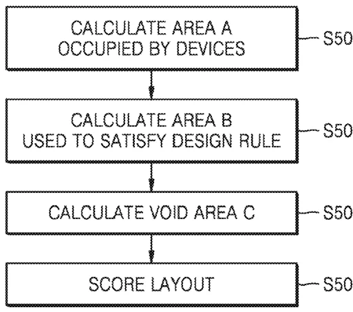
Samsung has been granted a patent for a method to design semiconductor layouts by scoring how much empty space exists between components. The system calculates the area needed for manufacturing processes and compares it to the actual space used to identify inefficient layouts. If the score indicates too much wasted space, the method rearranges the components to create a more compact final design.
In the filing’s own words
A method of designing a layout of a semiconductor device includes receiving an input layout of the device, scoring the input layout, determining whether to rearrange at least one device of the semiconductor device based on the scoring, and generating an output layout based on a rearrangement. The scoring includes calculating a first area occupied by one or more devices included in the semiconductor device in the input layout, calculating a second area of a manufacturing process based on a design rule for the one or more devices and the first area, calculating a void area of the input layout based on the first area and the second area, and calculating a score of the input layout based on the void area.
What exactly they claim (claim 1)
1. A method of designing a layout of a semiconductor device, the method comprising: receiving an input layout of the semiconductor device; scoring the input layout; determining whether to rearrange at least one device of the semiconductor device based on the scoring; and generating an output layout based on a rearrangement, wherein the scoring includes: calculating a first area occupied by one or more devices included in the semiconductor device in the input layout; calculating a second area required in a manufacturing process based on a design rule for the one or more devices and the first area; calculating a void area of the input layout based on the first area and the second area; and calculating a score of the input layout based on the void area.
Facts
- Company
- Samsung (Samsung Electronics Co., Ltd.)
- Official title
- Method of designing semiconductor device integrated circuit and layout thereof
- Patent number
- US12801825B2
- Application number
- 18465529
- Filed
- Sep 12, 2023
- Granted
- Nov 17, 2026
- Inventors
- 2
- Claims
- 20
Classified under
G06F 30/398 Physics & computingG06F 30/392 Physics & computingG06F 30/394 Physics & computingG06F 30/20 Physics & computingG06F 30/33 Physics & computingG06F 30/367 Physics & computingMore from Samsung in Chips & hardware
- Samsung patents quantum chip design using tiny electron traps Nov 12, 2026
- Samsung patents chip that combines camera and screen Oct 13, 2026
- Samsung patents chip that hides encrypted data from the main processor Oct 27, 2026
- Samsung patents display with tiny holes to hide cameras behind the screen Nov 3, 2026
- Samsung patents faster chip testing using machine learning Sep 1, 2026
Summaries are simplified from the filing’s own abstract and first claim. A patent filing is not a product announcement.
Patent data and drawings: U.S. Patent and Trademark Office (USPTO). Nebula is not affiliated with or endorsed by the USPTO.