Google patents software to automatically design light-guiding chips
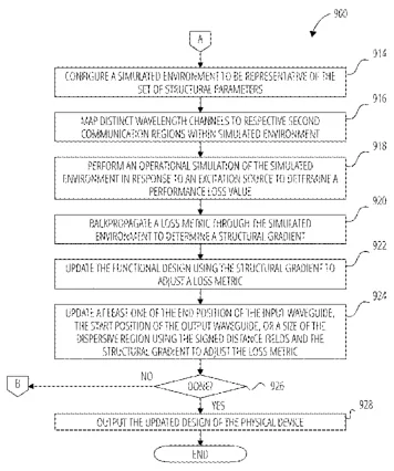
This patent describes a computer method that designs physical devices that guide light, such as those found in advanced chips. The software creates an initial layout of light paths and uses simulations to adjust the shape and size of these paths until they meet specific performance goals.
In the filing’s own words
In some embodiments, a computer-implemented method for designing a physical device is provided. A computing system generates an initial design that includes an input waveguide starting at an input location and extending to a end position, an output waveguide starting at a start position and extending to an output location, and a dispersive region. The computing system determines a set of structural parameters based on the initial design. The computing system simulates performance of the initial design using the set of structural parameters to determine a performance loss value based on at least one performance goal. The computing system updates at least one of the end position of the input waveguide, the start position of the output waveguide, or a size of the dispersive region in the initial design using a gradient of the performance loss value.
What exactly they claim (claim 1)
1. A non-transitory computer-readable medium having computer-executable instructions stored thereon that, in response to execution by one or more processors of a computing system, cause the computing system to perform actions for designing a physical device, the actions comprising: receiving, by the computing system, a design specification that includes an input location, an output location, and at least one performance goal; generating, by the computing system, an initial design based on the design specification, wherein the initial design includes an input waveguide starting at the input location and extending to an end position, an output waveguide starting at a start position and extending to the output location, and a dispersive region; determining, by the computing system, a set of structural parameters based on the initial design; simulating, by the computing system, performance of the initial design using the set of structural parameters to determine a performance loss value based on the at least one performance goal; and updating, by the computing system, at least one of the end position of the input waveguide, the start position of the output waveguide, or a size of the dispersive region in the initial design using a gradient of the performance loss value; wherein determining the set of structural parameters includes determining a signed distance field for the input waveguide, a signed distance field for the output waveguide, a signed distance field for the dispersive region, and a signed distance field for a functional design within the dispersive region.
Facts
- Company
- Google (X Development LLC)
- Official title
- Inverse design of photonic device footprints and waveguide locations
- Patent number
- US12801810B2
- Application number
- 18159006
- Filed
- Jan 24, 2023
- Granted
- Nov 17, 2026
- Inventors
- 2
- Claims
- 18
Classified under
G06F 30/20 Physics & computingG06F 2119/18 Physics & computingMore from Google in Chips & hardware
- Google patents radar network to track users across multiple devices Nov 10, 2026
- Google patents quantum gates to simulate particle physics Sep 1, 2026
- Waymo patents lidar chips that split light into multiple beams Sep 8, 2026
- Google patents chip design to speed up AI math tasks Sep 8, 2026
- Google patents display that turns off colors to save battery Sep 8, 2026
Summaries are simplified from the filing’s own abstract and first claim. A patent filing is not a product announcement.
Patent data and drawings: U.S. Patent and Trademark Office (USPTO). Nebula is not affiliated with or endorsed by the USPTO.