Google patents chip testing method that slows down signals to save time
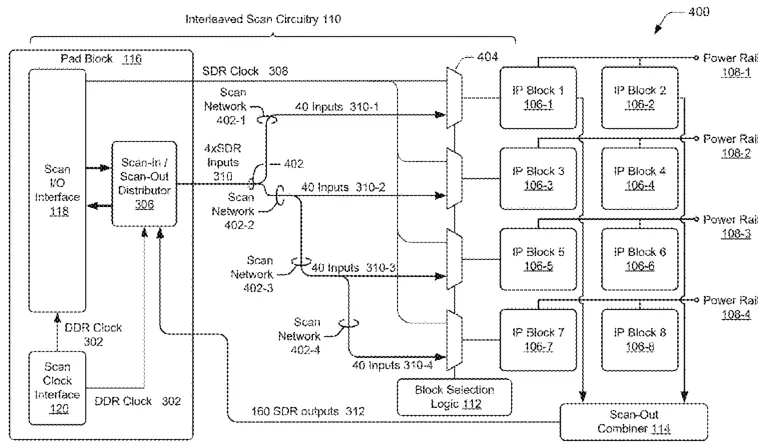
This patent describes a way to test computer chips by splitting the test signal into multiple slower streams. Instead of testing one part of the chip at a time, the system sends these slower signals to different parts simultaneously. This approach relaxes the speed requirements for the test equipment, making the process faster and cheaper.
In the filing’s own words
This document describes apparatuses and techniques for an interleaved scan architecture for concurrent testing of integrated circuit (IC) chips. In various aspects, an IC or system-on-chip may include interleaved scan circuitry, IP blocks or functional blocks on independent power rails, block selection logic, and a scan out combiner. The interleaved scan circuitry can receive test signaling that includes a set of test input/outputs (I/Os) at a first clock rate and generate, based on the received test signaling, multiple sets of test I/Os at a second clock rate for distribution to respective ones of the blocks. In some aspects, the second clock rate is lower than the first clock rate, which enables relaxing of timing constraints during testing and avoids usage of costly test-specific timing buffers. As such, the described aspects can reduce chip test time and reduce silicon complexity by avoiding the need for test-specific timing or power circuitry.
What exactly they claim (claim 1)
1. A system-on-chip comprising: power rails configured to provide power to components of the system-on-chip; intellectual property (IP) blocks; block selection logic configured to select, from the IP blocks, a group of multiple IP blocks that are each coupled to a different one of the power rails; and interleave scan circuitry configured to: receive test signaling comprising test input/outputs (I/Os) at a first clock rate; generate, based on the test signaling, multiple sets of test I/Os at a second clock rate that is different from the first clock rate; distribute each of the multiple sets of the test I/Os over a respective scan-in I/O bus to one of the IP blocks of the group of multiple IP blocks; and receive, over respective scan-out I/O buses and based on the multiple sets of test I/Os, multiple sets of result data from the group of multiple IP blocks.
Facts
- Company
- Google (Google LLC)
- Official title
- Interleaved scan architecture from concurrent testing
- Patent number
- US12801544B2
- Application number
- 19097464
- Filed
- Apr 1, 2025
- Granted
- Nov 17, 2026
- Inventors
- 4
- Claims
- 20
Classified under
G06F 13/20 Physics & computingG06F 1/04 Physics & computingG06F 2213/40 Physics & computingMore from Google in Chips & hardware
- Google patents radar network to track users across multiple devices Nov 10, 2026
- Google patents quantum gates to simulate particle physics Sep 1, 2026
- Waymo patents lidar chips that split light into multiple beams Sep 8, 2026
- Google patents chip design to speed up AI math tasks Sep 8, 2026
- Google patents display that turns off colors to save battery Sep 8, 2026
Summaries are simplified from the filing’s own abstract and first claim. A patent filing is not a product announcement.
Patent data and drawings: U.S. Patent and Trademark Office (USPTO). Nebula is not affiliated with or endorsed by the USPTO.