Samsung patents processor that fixes memory errors on the fly
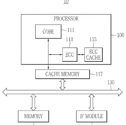
This patent describes a processor design that detects and corrects errors in instructions read from external memory. It stores the corrected instruction temporarily and sends it back to the memory only when the data bus is free, ensuring the processor executes the right command.
In the filing’s own words
A processor comprising an instruction fetch unit configured to read a first instruction stored in an external memory through a first data bus, generate a first correction instruction in which an error is corrected based on an error checking and correcting (ECC) operation for the first instruction, store an information for the first correction instruction, read a second instruction stored in the external memory through the first data bus according to a second instruction fetch, and transmit the first correction instruction to the external memory through the first data bus based on a flush condition, a decode unit configured to receive and decode the first correction instruction, and an execution unit configured to receive the decoded first correction instruction and execute an operation according to the first correction instruction.
What exactly they claim (claim 1)
1. A processor comprising: an instruction fetch circuit configured to read a first instruction stored in a memory through a first data bus according to a first instruction fetch in a first cycle, generate a first correction instruction configured to correct an error based on an error checking and correcting (ECC) operation, store information for the first correction instruction in the first cycle, read a second instruction stored in the memory through the first data bus according to a second instruction fetch in a second cycle after the first cycle while the information for the first correction instruction is stored, and transmit, in a third cycle after the second cycle, the first correction instruction to the memory through the first data bus based on a flush condition for transmitting the first correction instruction to the memory being satisfied, the flush condition representative of the first data bus being free of data transmission after the first cycle and the second cycle; a decode circuit configured to receive the first correction instruction and decode the first correction instruction; and an execution circuit configured to receive the decoded first correction instruction and execute an operation according to the first correction instruction.
Facts
- Company
- Samsung (SAMSUNG ELECTRONICS CO., LTD.)
- Official title
- Processor and memory system including the same
- Patent number
- US12801493B2
- Application number
- 18794447
- Filed
- Aug 5, 2024
- Granted
- Nov 17, 2026
- Inventors
- 6
- Claims
- 20
Classified under
G06F 11/1068 Physics & computingG06F 9/30047 Physics & computingG06F 9/3858 Physics & computingG06F 11/1016 Physics & computingMore from Samsung in Chips & hardware
- Samsung patents quantum chip design using tiny electron traps Nov 12, 2026
- Samsung patents chip that combines camera and screen Oct 13, 2026
- Samsung patents chip that hides encrypted data from the main processor Oct 27, 2026
- Samsung patents display with tiny holes to hide cameras behind the screen Nov 3, 2026
- Samsung patents faster chip testing using machine learning Sep 1, 2026
Summaries are simplified from the filing’s own abstract and first claim. A patent filing is not a product announcement.
Patent data and drawings: U.S. Patent and Trademark Office (USPTO). Nebula is not affiliated with or endorsed by the USPTO.