Samsung patents storage method to balance wear across memory sections
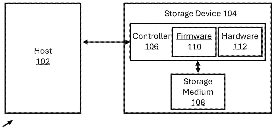
This patent describes a method for managing data storage by splitting a device's capacity into separate sections called domains. When a command is received, the controller checks the physical location of the data and reroutes the task to a different section if needed. This helps ensure that no single part of the storage wears out faster than the others.
In the filing’s own words
Methods and devices are provided in which a controller of a storage device receives a command. A logical capacity of the storage device is split into domains. The controller determines a logical address associated with the command. The logical address is associated with a first domain of the storage device. The command is rerouted from first resources of the controller attributed to the first domain to second resources of the controller attributed to a second domain of the storage device, based on a physical address associated with the logical address.
What exactly they claim (claim 1)
1. A method comprising: receiving a command at a controller of a storage device, wherein a logical capacity of the storage device is split into domains; determining, by the controller, a logical address associated with the command, wherein the logical address is associated with a first domain of the storage device; and rerouting the command from first resources of the controller attributed to the first domain to second resources of the controller attributed to a second domain of the storage device, based on a physical address associated with the logical address.
Facts
- Company
- Samsung (Samsung Electronics Co., Ltd.)
- Official title
- Method and device for backend wear level balancing of separated storage domains
- Patent number
- US12801288B2
- Application number
- 19084159
- Filed
- Mar 19, 2025
- Granted
- Nov 17, 2026
- Inventors
- 4
- Claims
- 20
Classified under
G06F 3/0616 Physics & computingG06F 3/0659 Physics & computingG06F 3/0679 Physics & computingMore from Samsung in Chips & hardware
- Samsung patents quantum chip design using tiny electron traps Nov 12, 2026
- Samsung patents chip that combines camera and screen Oct 13, 2026
- Samsung patents chip that hides encrypted data from the main processor Oct 27, 2026
- Samsung patents display with tiny holes to hide cameras behind the screen Nov 3, 2026
- Samsung patents faster chip testing using machine learning Sep 1, 2026
Summaries are simplified from the filing’s own abstract and first claim. A patent filing is not a product announcement.
Patent data and drawings: U.S. Patent and Trademark Office (USPTO). Nebula is not affiliated with or endorsed by the USPTO.