Samsung patents chip design that pauses clocks to save power
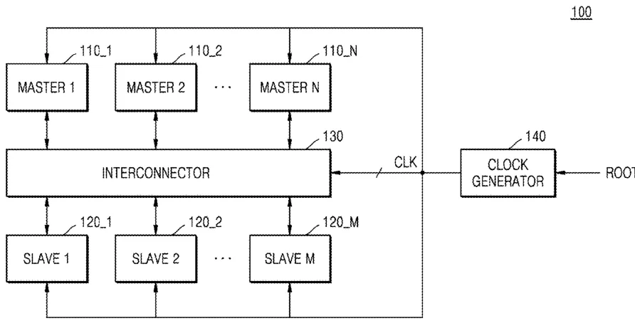
This patent describes a system on chip that uses control signals to turn off clock signals when data is not being actively sent between components. By pausing the clock during idle periods, the chip reduces unnecessary energy consumption.
In the filing’s own words
A system on chip includes interface nodes and clock gating cells. A first interface node outputs first and second control signals having a first bit value based on a first packet, outputs the first packet based on a first clock signal, and outputs the first and second control signals having a second bit value based on first packet transmission. A second interface node outputs a third control signal in response to handshaking the first interface node, and receives the first packet from the first interface node based on a second clock signal. A first clock gating cell outputs the first clock signal based on an external clock signal and gates the first clock signal based on the first control signal. A second clock gating cell outputs the second clock signal based on the external clock signal and gates the second clock signal based on the second and third control signals.
What exactly they claim (claim 1)
1. A system on chip, comprising: a first interface node configured to output a first clock control signal and a second clock control signal each having a first bit value, based on a first packet received from a first semiconductor Intellectual Property (IP), output the first packet, based on a first clock signal, and output the first clock control signal and the second clock control signal each having a second bit value, based on a determination that transmission of the first packet from the first interface node is completed; a second interface node configured to output a third clock control signal having the first bit value in response to handshaking with the first interface node, and receive the first packet from the first interface node, based on a second clock signal; a first clock gating cell configured to output the first clock signal, based on an external clock signal received from an external signal source, the external signal source external to the first clock gating cell, and gate the first clock signal, based on the first clock control signal; and a second clock gating cell configured to output the second clock signal, based on the external clock signal, and gate the second clock signal, based on the second clock control signal and the third clock control signal.
Facts
- Company
- Samsung (Samsung Electronics Co., Ltd.)
- Official title
- System on chip and operating method thereof for selectively gating clock signal in low utilization
- Patent number
- US12801177B2
- Application number
- 18933254
- Filed
- Oct 31, 2024
- Granted
- Nov 17, 2026
- Inventors
- 4
- Claims
- 8
Classified under
G06F 1/08 Physics & computingG06F 1/12 Physics & computingH03K 19/20 Electricity & electronicsMore from Samsung in Chips & hardware
- Samsung patents quantum chip design using tiny electron traps Nov 12, 2026
- Samsung patents chip that combines camera and screen Oct 13, 2026
- Samsung patents chip that hides encrypted data from the main processor Oct 27, 2026
- Samsung patents display with tiny holes to hide cameras behind the screen Nov 3, 2026
- Samsung patents faster chip testing using machine learning Sep 1, 2026
Summaries are simplified from the filing’s own abstract and first claim. A patent filing is not a product announcement.
Patent data and drawings: U.S. Patent and Trademark Office (USPTO). Nebula is not affiliated with or endorsed by the USPTO.