Samsung patents chip manufacturing method using dual alignment marks
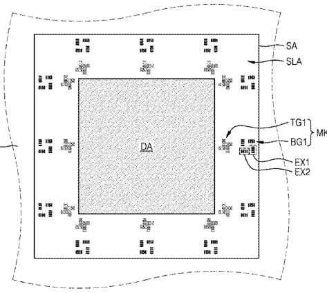
This patent describes a way to make computer chips by using two separate alignment patterns, or 'gratings,' on the lower layers of the device. The method averages the alignment data from both patterns to create a more accurate baseline for checking how well the top layers line up.
In the filing’s own words
A method of manufacturing an integrated circuit device, includes: forming a bottom metrology mark; determining a bottom grating integrated measurement value, based on a first average value of a first alignment measurement value for a first bottom grating and a second alignment measurement value for a second bottom grating, wherein the first alignment measurement value and the second alignment measurement value are measured on the bottom metrology mark; forming a top grating including a plurality of third keys formed at a third vertical level that is higher than each of the first vertical level and the second vertical level on the lower structure; and measuring an overlay between the top grating and both of the first bottom grating and the second bottom grating, based on a measurement value of the top grating and based on the bottom grating integrated measurement value.
What exactly they claim (claim 1)
1. A method of manufacturing an integrated circuit device, the method comprising: forming a bottom metrology mark that comprises: a first bottom grating including a plurality of first keys, and a second bottom grating including a plurality of second keys, wherein the plurality of first keys are formed at a first vertical level on a lower structure and at a first time instance, and wherein the plurality of second keys are formed, at the first vertical level on the lower structure or at a second vertical level that is higher than the first vertical level, at a second time instance that is different from the first time instance; determining a bottom grating integrated measurement value, based on a first average value of a first alignment measurement value for the first bottom grating and a second alignment measurement value for the second bottom grating, wherein the first alignment measurement value and the second alignment measurement value are measured on the bottom metrology mark; forming a top grating including a plurality of third keys that are formed at a third vertical level that is higher than each of the first vertical level and the second vertical level on the lower structure; and measuring an overlay between the top grating and both of the first bottom grating and the second bottom grating, based on a measurement value of the top grating and based on the bottom grating integrated measurement value.
Facts
- Company
- Samsung (SAMSUNG ELECTRONICS CO., LTD.)
- Official title
- Method of manufacturing integrated circuit device by using metrology mark for photolithography process
- Patent number
- US12801032B2
- Application number
- 19173298
- Filed
- Apr 8, 2025
- Granted
- Nov 17, 2026
- Inventors
- 6
- Claims
- 20
Classified under
G03F 7/70633 Physics & computingG03F 7/70683 Physics & computingG03F 7/706845 Physics & computingG03F 7/706849 Physics & computingH10W 20/031 Electricity & electronicsMore from Samsung in Chips & hardware
- Samsung patents quantum chip design using tiny electron traps Nov 12, 2026
- Samsung patents chip that combines camera and screen Oct 13, 2026
- Samsung patents chip that hides encrypted data from the main processor Oct 27, 2026
- Samsung patents display with tiny holes to hide cameras behind the screen Nov 3, 2026
- Samsung patents faster chip testing using machine learning Sep 1, 2026
Summaries are simplified from the filing’s own abstract and first claim. A patent filing is not a product announcement.
Patent data and drawings: U.S. Patent and Trademark Office (USPTO). Nebula is not affiliated with or endorsed by the USPTO.