Samsung patents display wiring that links two control chips together
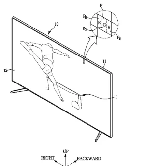
Samsung describes a display panel design that uses two separate control chips, known as Chip On Film (COF), to drive the pixels on a screen. The filing details a specific layout where a 'dummy' section between the two chips contains a conductive pattern that electrically connects them. This setup allows the two chips to share signals through dummy pins, which helps manage the data needed to light up the display.
In the filing’s own words
A display apparatus includes a substrate including an active area including a plurality of pixels, and an outer lead bonding (OLB) area; a first Chip On Film (COF) coupled to the OLB area; a second COF coupled to the OLB area and adjacent to the first COF; a first printed circuit board (PCB) coupled to the first COF; and a second PCB coupled to the second COF, wherein the OLB area may include a first area to which the first COF is coupled, a second area to which the second COF is coupled, and a dummy area between the first area and the second area, and the dummy area may include a conductive pattern electrically connecting the first COF and the second COF.
What exactly they claim (claim 1)
1. A display panel comprising: a substrate comprising an active area comprising a plurality of pixels, and an outer lead bonding (OLB) area; a first Chip On Film (COF) coupled to the OLB area; a second COF coupled to the OLB area and adjacent to the first COF; a first printed circuit board (PCB) coupled to the first COF; and a second PCB coupled to the second COF, wherein the OLB area comprises a first area to which the first COF is coupled, a second area to which the second COF is coupled, and a dummy area between the first area and the second area, and wherein the dummy area comprises a conductive pattern electrically connecting the first COF and the second COF, wherein each of the first COF and the second COF comprises: a plurality of signal pins configured to output signals for driving the plurality of pixels; and a plurality of dummy pins, and wherein the plurality of dummy pins of the first COF are electrically connected to the plurality of dummy pins of the second COF through the conductive pattern.
Facts
- Company
- Samsung (SAMSUNG ELECTRONICS CO., LTD.)
- Official title
- Display panel, display apparatus including display panel, and method for manufacturing display panel
- Patent number
- US12800968B2
- Application number
- 18391148
- Filed
- Dec 20, 2023
- Granted
- Nov 17, 2026
- Inventors
- 2
- Claims
- 13
Classified under
G02F 1/13452 Physics & computingH10D 86/441 Electricity & electronicsH10D 86/60 Electricity & electronicsG02F 1/136286 Physics & computingG02F 1/1368 Physics & computingH10W 70/611 Electricity & electronicsMore from Samsung in Chips & hardware
- Samsung patents quantum chip design using tiny electron traps Nov 12, 2026
- Samsung patents chip that combines camera and screen Oct 13, 2026
- Samsung patents chip that hides encrypted data from the main processor Oct 27, 2026
- Samsung patents display with tiny holes to hide cameras behind the screen Nov 3, 2026
- Samsung patents faster chip testing using machine learning Sep 1, 2026
Summaries are simplified from the filing’s own abstract and first claim. A patent filing is not a product announcement.
Patent data and drawings: U.S. Patent and Trademark Office (USPTO). Nebula is not affiliated with or endorsed by the USPTO.