Samsung patents IR sensor using doped phase-change material
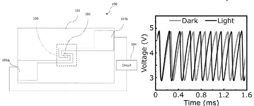
Samsung describes an infrared sensor that uses a thin layer of phase-change material mixed with tungsten to detect heat radiation. When infrared light hits the layer, it changes the frequency of an electrical signal generated by the material, which the sensor's circuit then measures.
In the filing’s own words
An IR sensor comprises a substrate, a rear reflector on the substrate, a supporting layer, a PCM layer carried by the supporting layer and comprising a PCM material, and a second dopant material different than the PCM material, and first and second electrically conductive contacts carried by the substrate and coupled to opposing sides of the PCM layer. The IR sensor also includes a circuit coupled to the first and second electrically conductive contacts and configured to apply an electrical bias signal to the PCM layer to generate an electrical oscillation, and detect the frequency modulation (FM) of the oscillation signal based upon IR radiation received by the PCM layer.
What exactly they claim (claim 1)
1. An infrared (IR) sensor comprising: a substrate; a rear reflector on the substrate; a support layer carried by the substrate; a phase change material (PCM) layer carried by the support layer and comprising a PCM material, and a second dopant material different than the PCM material, the second dopant material comprising tungsten, the PCM layer having a grain size within a range of 10-100 nanometers; first and second electrically conductive contacts carried by the substrate and coupled to opposing sides of the PCM layer; and a circuit coupled to the first and second electrically conductive contacts and configured to apply an electrical bias signal to the PCM layer to cause an oscillation signal to be generated within the PCM layer, and detect frequency changes in the oscillation signal based upon IR radiation received by the PCM layer.
Facts
- Company
- Samsung (SAMSUNG ELECTRONICS CO., LTD.)
- Official title
- Frequency modulation based IR with doped PCM layer and related methods
- Patent number
- US12800400B2
- Application number
- 19053586
- Filed
- Feb 14, 2025
- Granted
- Nov 17, 2026
- Inventors
- 4
- Claims
- 20
Classified under
G01J 5/24 Physics & computingG01J 5/0225 Physics & computingG01J 5/34 Physics & computingMore from Samsung in Chips & hardware
- Samsung patents quantum chip design using tiny electron traps Nov 12, 2026
- Samsung patents chip that combines camera and screen Oct 13, 2026
- Samsung patents chip that hides encrypted data from the main processor Oct 27, 2026
- Samsung patents display with tiny holes to hide cameras behind the screen Nov 3, 2026
- Samsung patents faster chip testing using machine learning Sep 1, 2026
Summaries are simplified from the filing’s own abstract and first claim. A patent filing is not a product announcement.
Patent data and drawings: U.S. Patent and Trademark Office (USPTO). Nebula is not affiliated with or endorsed by the USPTO.