Nvidia patents method to stabilize chip timing against power noise
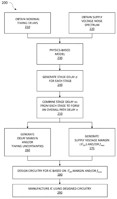
Nvidia describes a design process that calculates how power supply fluctuations affect the speed of different parts of a chip. By using a mathematical model to predict these timing delays, engineers can set a specific voltage margin to ensure the circuit operates reliably.
In the filing’s own words
A method of designing and manufacturing an integrated circuit (IC), is disclosed. In one embodiment, the method comprises obtaining a nominal delay for each of a plurality of portions of the IC and obtaining a noise spectrum across frequency for a voltage supplied to the IC (V DD). The method further comprises inputting the nominal delay for each of the plurality of portions of the IC and the noise spectrum across frequency for V DD into a physics-based mathematical model where the model generates a statistical standard deviation (σ) for a delay for each of the plurality of portions of the IC at each noise frequency band of the noise spectrum for V DD (delay σ) and the delay σs are combined IC into an overall delay σ. The method further comprises determining a margin of V DD that compensates for the noise spectrum based on the overall delay σ.
What exactly they claim (claim 1)
1. A method of designing and manufacturing an integrated circuit (IC), the method comprising: obtaining a nominal delay for each of a plurality of portions of the IC, the nominal delay not including any noise characteristics for each of the plurality of portions of the IC; obtaining a noise spectrum across frequency for a voltage supplied to the IC (V DD); inputting the nominal delay for each of the plurality of portions of the IC and the noise spectrum across frequency for V DD into a physics-based mathematical model (model); generating, by the model, a statistical standard deviation (σ) for a delay for each of the plurality of portions of the IC at each noise frequency band of the noise spectrum for V DD (delay σ); combining delay σs for each of the plurality of portions of the IC into an overall delay σ; determining a margin of V DD that compensates for the noise spectrum based on the overall delay σ; designing circuitry for the IC based on the V DD margin; and manufacturing the IC using the designed circuitry.
Facts
- Company
- Nvidia (NVIDIA Corporation)
- Official title
- METHOD TO COMPENSATE SUPPLY VOLTAGE FLUCTUATION IN AN INTEGRATED CIRCUIT
- Publication number
- US20260359541A1
- Application number
- 19201444
- Filed
- May 7, 2025
- Published
- Nov 12, 2026
- Inventors
- 7
- Claims
- 19
Classified under
G06F 30/367 Physics & computingG06F 30/373 Physics & computingG06F 2111/10 Physics & computingG06F 2119/10 Physics & computingG06F 2119/12 Physics & computingMore from Nvidia in Chips & hardware
- Nvidia stacks memory directly on chips to boost data speed Nov 10, 2026
- Nvidia patents method to skip zero data in neural network math Oct 13, 2026
- Nvidia patents hardware to speed up motion blur in ray tracing Oct 13, 2026
- Nvidia patents method to sync data across split processor chips Sep 17, 2026
- Nvidia patents chip math trick to speed up AI calculations Oct 8, 2026
Summaries are simplified from the filing’s own abstract and first claim. A patent filing is not a product announcement.
Patent data and drawings: U.S. Patent and Trademark Office (USPTO). Nebula is not affiliated with or endorsed by the USPTO.