Tesla patents chip assembly that fixes uneven cooling contact
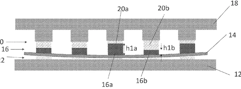
Tesla describes a method for building computer chips where the base wafer is slightly curved. The design uses a special structure to adjust the height of electronic modules so they sit flush against the cooling system, ensuring heat is removed effectively.
In the filing’s own words
Wafer assemblies and related methods of manufacture are disclosed. Such assemblies and methods can account for different heights of electronic modules positioned on a wafer. In an embodiment, a wafer assembly includes a cooling system, a wafer, a first electronic module, a second electronic module, and a height adjustment structure. A first thermal interface material (TIM) can be disposed between the first electronic module and a first portion of the cooling system. A second TIM can be disposed between the second electronic module and a second portion of the cooling system. The height adjustment structure can compensate for a height difference between the first electronic module and the second electronic module. Other wafer assemblies and methods of manufacture are disclosed.
What exactly they claim (claim 1)
1. A wafer assembly comprising: a cooling system; a wafer; a first electronic module mounted on a first location of the wafer and coupled to a first portion of the cooling system, the first electronic module and the first portion of the cooling system positioned such that a first thermal interface material (TIM) is disposed between the first electronic module and the first portion of the cooling system; a second electronic module mounted on a second location of the wafer different from the first location and coupled to a second portion of the cooling system, the second electronic module and the second portion of the cooling system positioned such that a second TIM is disposed between the second electronic module and the second portion of the cooling system, wherein the wafer is curved such that the first location is a different distance from the cooling system than the second location; and a height adjustment structure disposed between the first location of the wafer and the first portion of the cooling system, the height adjustment structure configured to compensate for a height difference between the first electronic module and the second electronic module.
Facts
- Company
- Tesla (Tesla, Inc.)
- Official title
- Electronic assemblies and methods of manufacturing the same
- Patent number
- US12805312B2
- Application number
- 18576230
- Filed
- Jun 28, 2022
- Granted
- Nov 17, 2026
- Inventors
- 5
- Claims
- 20
Classified under
H10W 40/22 Electricity & electronicsH10W 40/037 Electricity & electronicsH10W 40/60 Electricity & electronicsMore from Tesla in Chips & hardware
- Tesla patents chip cooling system that blocks static and interference Nov 17, 2026
- Tesla patents method to detect dangerous electrical arcs in vehicle systems Oct 8, 2026
- Tesla patents flexible 3D touch sensors that bend to fit curved surfaces Oct 8, 2026
- Tesla patents conductive grease to ground electric drivetrain bearings Sep 22, 2026
- Tesla patents single-wire control for lit buttons and switches Sep 22, 2026
Summaries are simplified from the filing’s own abstract and first claim. A patent filing is not a product announcement.
Patent data and drawings: U.S. Patent and Trademark Office (USPTO). Nebula is not affiliated with or endorsed by the USPTO.