Sony patents camera sensor that sharpens focus using split light data
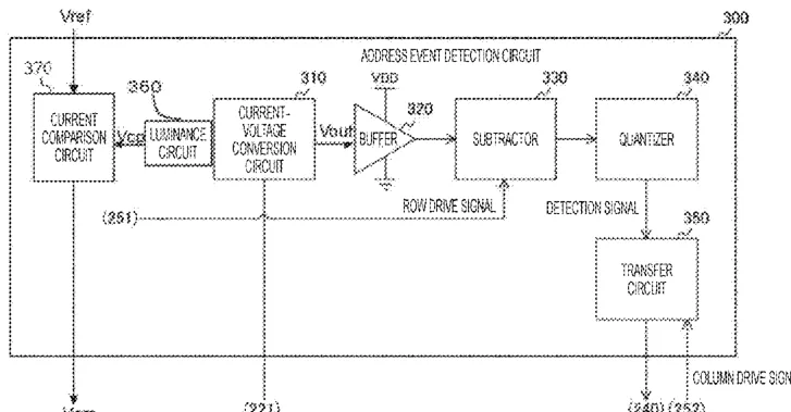
Sony describes a photodetection device that splits incoming light between two sets of pixels to measure focus accuracy. By comparing the brightness signals from these paired pixels, the system calculates how far the lens needs to move to make the image sharp.
In the filing’s own words
Event-based vision sensors that support image plane phase difference method AF functions are disclosed. In one example, a photodetection device includes first and second pixels respectively configured to photoelectrically convert incident light from one side and an opposite side to generate first and second currents. First and second luminance circuits respectively corresponding to the first and second pixels generate first and second luminance signals, and first and second current comparison circuits respectively corresponding to the first and second pixels compare the first and second luminance signals with a reference signal and convert them into first and second digital signals. A controller adjusts a focal position of the incident light on the basis of the first digital signal and the second digital signal.
What exactly they claim (claim 1)
1. A photodetection device comprising: a plurality of first pixels configured to photoelectrically convert incident light from a portion on one side to generate a first current; a plurality of second pixels configured to photoelectrically convert the incident light from a portion on a side opposite to the portion on the one side of each of the first pixels to generate a second current; a plurality of first luminance circuits provided individually corresponding to the plurality of first pixels and configured to generate a first luminance signal according to the first current; a plurality of second luminance circuits provided individually corresponding to the plurality of second pixels and configured to generate a second luminance signal according to the second current; a plurality of first current comparison circuits provided individually corresponding to the plurality of first pixels, and configured to compare the first luminance signal with a reference signal and convert the first luminance signal into a first digital signal; a plurality of second current comparison circuits provided individually corresponding to the plurality of second pixels, and configured to compare the second luminance signal with the reference signal and convert the second luminance signal into a second digital signal; and a control unit configured to adjust a focal position of the incident light on a basis of the first digital signal and the second digital signal.
Facts
- Company
- Sony (Sony Semiconductor Solutions Corporation)
- Official title
- Photodetection device
- Patent number
- US12804280B2
- Application number
- 18711246
- Filed
- Nov 14, 2022
- Granted
- Nov 17, 2026
- Inventors
- 1
- Claims
- 17
Classified under
H04N 25/704 Electricity & electronicsH04N 25/47 Electricity & electronicsH04N 25/77 Electricity & electronicsMore from Sony in Cameras & imaging
- Sony patents camera chips that sign photos to prove they are real Sep 15, 2026
- Sony patents camera sensor design to boost image range without slowing video Oct 29, 2026
- Sony patents camera setup that learns to mimic a virtual view Sep 1, 2026
- Sony patents camera method to reduce lag in burst mode photos Sep 1, 2026
- Sony patents camera sensor design to improve global shutter image quality Sep 1, 2026
Summaries are simplified from the filing’s own abstract and first claim. A patent filing is not a product announcement.
Patent data and drawings: U.S. Patent and Trademark Office (USPTO). Nebula is not affiliated with or endorsed by the USPTO.