Sony patents camera sensor that combines two light types to reduce noise
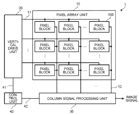
Sony describes an imaging element with two types of pixels that capture light at different wavelengths. The sensor can combine the signals from both pixels to create a clearer image or subtract one from the other to isolate specific light details.
In the filing’s own words
Imaging with reduced noise is disclosed. In one example, an imaging element includes a pixel block including a first pixel and a second pixel that performs photoelectric conversion of incident light of a wavelength different from that of the first pixel. An electric charge holding unit holds electric charges of the first and second pixels, and a signal generation unit generates an image signal based on the held electric charges. A pixel block controller controls transfer of the electric charges of the first pixel to generate a first image signal and of the second pixel to generate an added image signal. A signal processing unit switches a first mode for outputting the first image signal and the added image signal and a second mode for outputting the first image signal and a second image signal obtained by subtracting the first image signal from the added image signal.
What exactly they claim (claim 1)
1. An imaging element comprising: a pixel block including a first pixel that performs photoelectric conversion of incident light having a predetermined wavelength among kinds of incident light and generates electric charges, a second pixel that performs photoelectric conversion of incident light having a wavelength different from the wavelength of the first pixel and generates electric charges, an electric charge holding unit that holds the electric charges generated by the first pixel and the second pixel, and a signal generation circuit that generates an image signal based on the electric charges held by the electric charge holding unit; a pixel block control circuit that performs control to transfer the electric charges generated by the first pixel to the electric charge holding unit and cause the signal generation circuit to generate a first image signal that is the image signal based on the electric charges and control to further transfer the electric charges generated by the second pixel to the electric charge holding unit in which the electric charges generated by the first pixel are held and cause the signal generation circuit to generate an added image signal that is the image signal based on electric charges obtained by adding up the electric charges respectively generated by the first pixel and the second pixel; and a signal processor configured to generate a second image signal that is the image signal obtained by subtracting the first image signal from the added image signal, the signal processor switching a first mode for outputting the first image signal and the added image signal and a second mode for outputting the first image signal and the second image signal wherein the first pixel includes a plurality of photoelectric conversion units for subjecting a subject to pupil division, and the pixel block control circuit further performs control to transfer electric charges generated by any one of the plurality of photoelectric conversion units of the first pixel to the electric charge holding unit and cause the signal generation circuit to generate an image signal based on the electric charges, and transfers electric charges generated by the plurality of photoelectric conversion units of the first pixel to the electric charge holding unit and causes the signal generation circuit to generate an image signal based on the electric charges as the first image signal.
Facts
- Company
- Sony (Sony Semiconductor Solutions Corporation)
- Official title
- Imaging element and electronic equipment
- Patent number
- US12804279B2
- Application number
- 18730426
- Filed
- Nov 16, 2022
- Granted
- Nov 17, 2026
- Inventors
- 2
- Claims
- 6
Classified under
H04N 25/673 Electricity & electronicsH04N 25/136 Electricity & electronicsH04N 25/78 Electricity & electronicsMore from Sony in Cameras & imaging
- Sony patents camera chips that sign photos to prove they are real Sep 15, 2026
- Sony patents camera sensor design to boost image range without slowing video Oct 29, 2026
- Sony patents camera setup that learns to mimic a virtual view Sep 1, 2026
- Sony patents camera method to reduce lag in burst mode photos Sep 1, 2026
- Sony patents camera sensor design to improve global shutter image quality Sep 1, 2026
Summaries are simplified from the filing’s own abstract and first claim. A patent filing is not a product announcement.
Patent data and drawings: U.S. Patent and Trademark Office (USPTO). Nebula is not affiliated with or endorsed by the USPTO.