Samsung patents stacked LED display with specific material doping
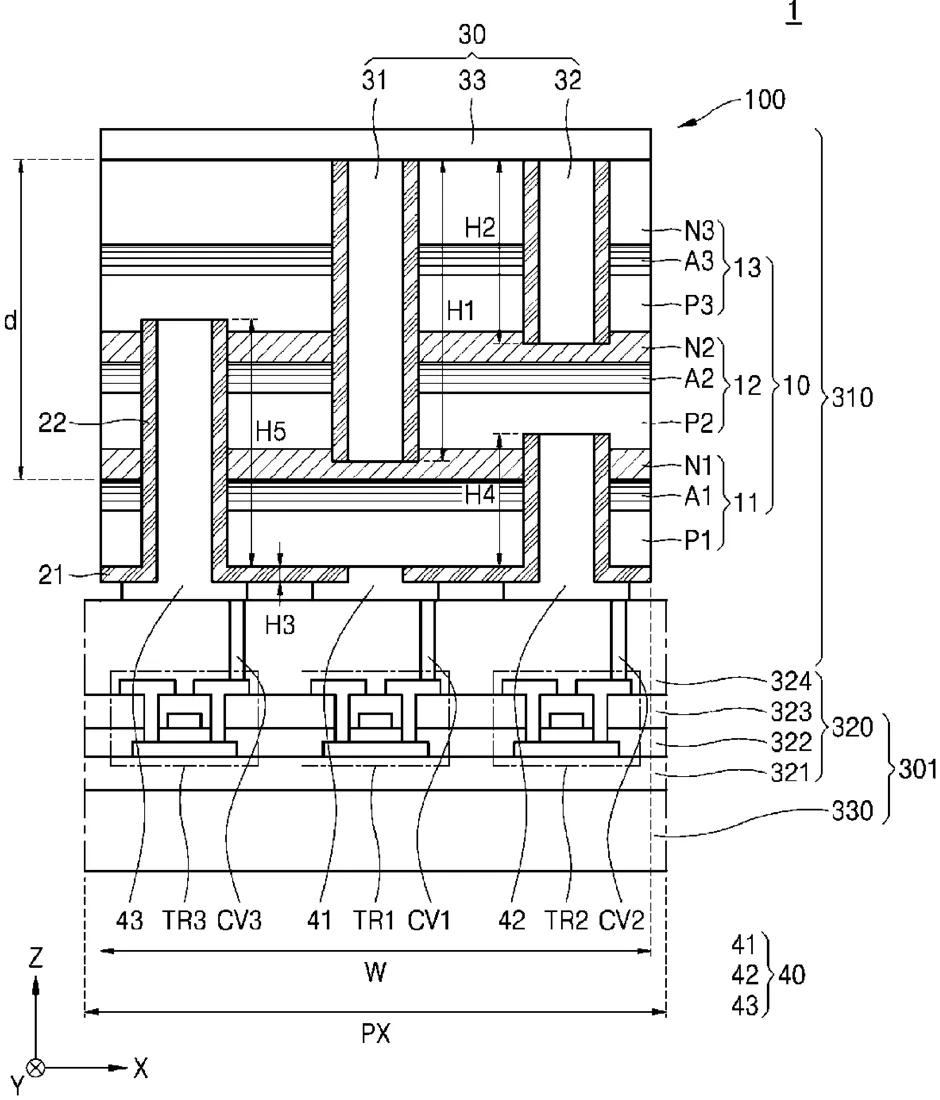
Samsung describes a display technology where three light-emitting elements are stacked vertically on top of each other within a single pixel. Each element is made of semiconductor layers designed to emit light at different wavelengths, allowing them to produce different colors. The filing specifies that the bottom layer uses a material called AlGaN with a high concentration of electrical impurities to control how it conducts electricity.
In the filing’s own words
A display apparatus includes a display layer including a plurality of light-emitting devices, and a drive layer configured to drive the plurality of light-emitting devices, where at least one of the plurality of light-emitting devices includes a light-emitting structure including a first light-emitting element, a second light-emitting element, and a third light-emitting element sequentially and monolithically stacked from the drive layer in a first direction, each of the first light-emitting element, the second light-emitting element, and the third light-emitting element including a p-type semiconductor layer, an active layer, and an n-type semiconductor layer, where the n-type semiconductor layer of the first light-emitting element includes AlGaN and a doping amount of an n-type dopant in the n-type semiconductor layer of the first light-emitting element is 2E+19/cm 3 or more.
What exactly they claim (claim 1)
1. A display apparatus comprising: a display layer comprising a plurality of light-emitting devices; and a drive layer configured to drive the plurality of light-emitting devices, wherein at least one of the plurality of light-emitting devices comprises: a light-emitting structure comprising a first light-emitting element, a second light-emitting element, and a third light-emitting element sequentially and monolithically stacked from the drive layer in a first direction, each of the first light-emitting element, the second light-emitting element, and the third light-emitting element comprising a p-type semiconductor layer, an active layer, and an n-type semiconductor layer, and being respectively configured to emit light of different wavelengths, a first electrode pattern connected to the n-type semiconductor layer of the first light-emitting element, the n-type semiconductor layer of the second light-emitting element, and the n-type semiconductor layer of the third light-emitting element, and a second electrode pattern electrically connected to the p-type semiconductor layer of the first light-emitting element, the p-type semiconductor layer of the second light-emitting element, and the p-type semiconductor layer of the third light-emitting element, wherein the n-type semiconductor layer of the first light-emitting element comprises AlGaN, and wherein a doping amount of an n-type dopant in the n-type semiconductor layer of the first light-emitting element is 2E+19/cm 3 or more.
Facts
- Company
- Samsung (SAMSUNG ELECTRONICS CO., LTD.)
- Official title
- DISPLAY APPARATUS AND METHOD OF MANUFACTURING THE SAME
- Publication number
- US20260333978A1
- Application number
- 19465554
- Filed
- Jan 30, 2026
- Published
- Oct 22, 2026
- Inventors
- 5
- Claims
- 20
Classified under
H10H 29/8321 Electricity & electronicsH10H 20/825 Electricity & electronicsH10H 29/012 Electricity & electronicsH10H 29/39 Electricity & electronicsMore from Samsung in Chips & hardware
- Samsung patents chip that combines camera and screen Oct 13, 2026
- Samsung patents faster chip testing using machine learning Sep 1, 2026
- Samsung patents radar method to pinpoint target direction more accurately Sep 1, 2026
- Samsung patents memory chip that searches data by content, not address Sep 1, 2026
- Samsung patents chip design that skips empty data to speed up AI Sep 1, 2026
Summaries are simplified from the filing’s own abstract and first claim. A patent filing is not a product announcement.
Patent data and drawings: U.S. Patent and Trademark Office (USPTO). Nebula is not affiliated with or endorsed by the USPTO.