Samsung patents chip design with new gate spacing method
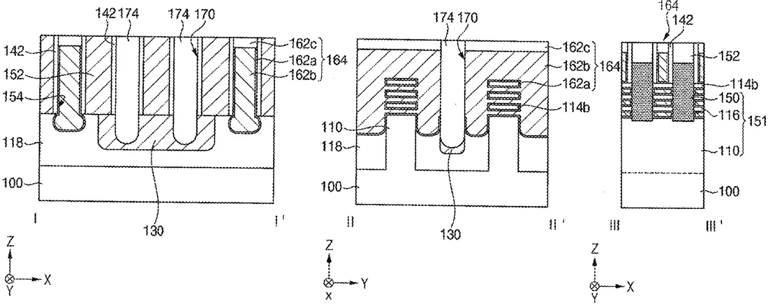
Samsung has filed a patent for a method to build semiconductor devices, specifically field effect transistors, which are the tiny switches inside computer chips. The design uses a specific sequence of steps to create gate structures and fill the gaps between them with insulation to improve the device's layout.
In the filing’s own words
The present disclosure provides for semiconductor devices including field effect transistors. In some embodiments, the semiconductor device includes active structures extending in a first direction on a substrate, an isolation pattern formed in a trench between the active structures, gate structures extending in a second direction across the active structures, a cutting insulation pattern formed between end portions of the gate structures in the second direction, and a lower impurity region at an upper portion of the isolation pattern. A first shape of a lower portion of the cutting insulation pattern disposed under an uppermost surface of the isolation pattern is different from a second shape of a lower portion of the gate structures disposed under the uppermost surface of the isolation pattern. The gate structures are formed on the active structures and the isolation pattern. The lower impurity region contacts at least a portion of the cutting insulation pattern.
What exactly they claim (claim 1)
1. A method for manufacturing a semiconductor device, comprising: forming preliminary active structures on a substrate, the preliminary active structures extending in a first direction and spaced apart in a second direction perpendicular to the first direction; forming an isolation pattern at least partially covering lower sidewalls of the preliminary active structures; forming a lower impurity region on the isolation pattern between the preliminary active structures; forming active structures by removing a portion of the preliminary active structures; forming a preliminary gate structure on the active structures, the isolation pattern, and the lower impurity region, the preliminary gate structure extending in the second direction and crossing channel structures, the isolation pattern, and the lower impurity region; forming a plurality of gate structures by cutting the portion of the preliminary gate structure disposed on the lower impurity region, the plurality of gate structures having first end portions facing each other in the second direction; and forming a cutting insulation pattern by filling openings between the first end portions of the plurality of gate structures.
Facts
- Company
- Samsung (SAMSUNG ELECTRONICS CO., LTD.)
- Official title
- SEMICONDUCTOR DEVICE
- Publication number
- US20260333761A1
- Application number
- 19468556
- Filed
- Feb 3, 2026
- Published
- Oct 22, 2026
- Inventors
- 5
- Claims
- 20
Classified under
H10D 30/6735 Electricity & electronicsH10D 30/43 Electricity & electronicsH10D 30/6757 Electricity & electronicsH10D 62/121 Electricity & electronicsMore from Samsung in Chips & hardware
- Samsung patents chip that combines camera and screen Oct 13, 2026
- Samsung patents faster chip testing using machine learning Sep 1, 2026
- Samsung patents radar method to pinpoint target direction more accurately Sep 1, 2026
- Samsung patents memory chip that searches data by content, not address Sep 1, 2026
- Samsung patents chip design that skips empty data to speed up AI Sep 1, 2026
Summaries are simplified from the filing’s own abstract and first claim. A patent filing is not a product announcement.
Patent data and drawings: U.S. Patent and Trademark Office (USPTO). Nebula is not affiliated with or endorsed by the USPTO.