Samsung patents memory chip design using ferroelectric layers
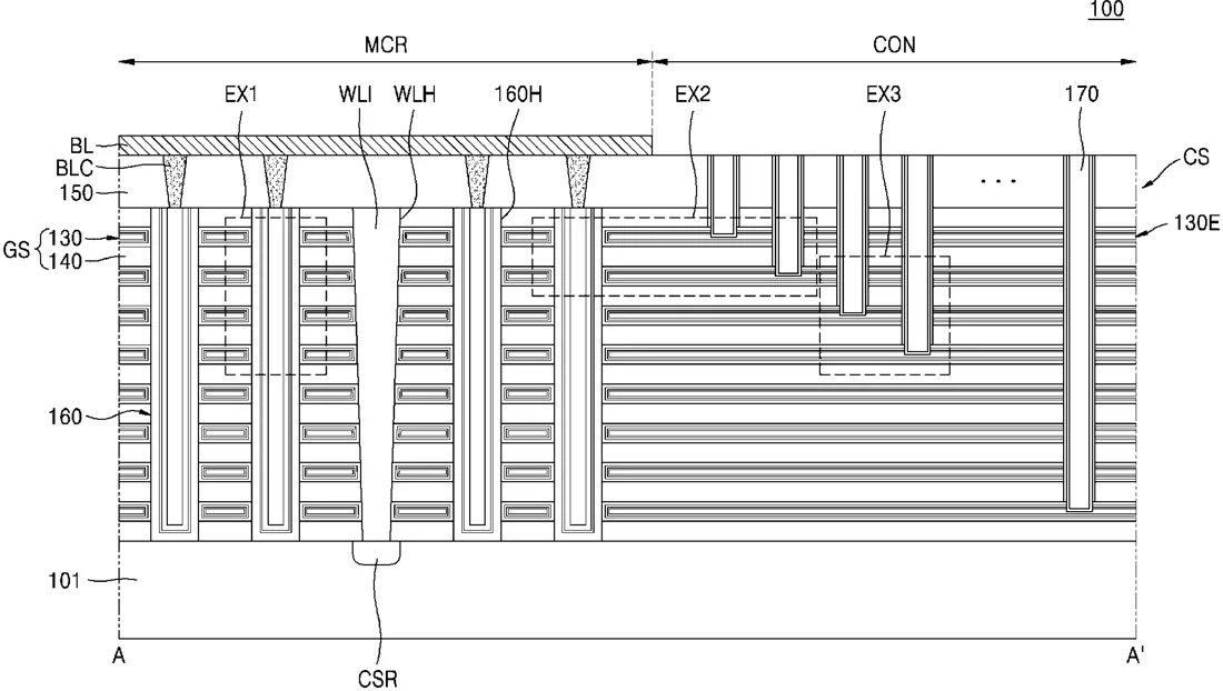
Samsung has filed a patent for a semiconductor device that uses a specific arrangement of insulating layers to improve electrical performance. The design incorporates ferroelectric materials in the channel structures, which are components that help store data in memory chips.
In the filing’s own words
The present disclosure relates to a semiconductor device. In an example semiconductor device, a gate insulating layer is formed in a structure other than a channel structure, and thus, the gate insulating layer having a small thickness may be formed relatively easily, thereby improving electrical characteristics of the semiconductor device. In addition, when forming a plurality of plug structures in a stepped configuration in a connection region, a gate insulating layer extension may be used as an etch stop layer. Accordingly, the semiconductor device may reduce a process variation of a stair-free contact structure, even when the number of layers of word lines increases.
What exactly they claim (claim 1)
1. A semiconductor device comprising: a plurality of conductive line structures extending in a horizontal direction above a semiconductor substrate, the plurality of conductive line structures overlapping each other in a vertical direction, wherein the semiconductor substrate comprises a memory cell region and a connection region; a plurality of insulating layers, each insulating layer of the plurality of insulating layers being located between two neighboring conductive line structures of the plurality of conductive line structures, and the plurality of insulating layers extending in the horizontal direction; a plurality of channel structures extending in the vertical direction through the plurality of conductive line structures and the plurality of insulating layers in the memory cell region; and a plurality of plug structures having different heights in the connection region, the plurality of plug structures extending in the vertical direction, and the plurality of plug structures respectively corresponding to the plurality of conductive line structures, wherein each channel structure of the plurality of channel structures comprises a ferroelectric layer, a channel-side dielectric layer, a channel layer, and an insulating plug that are sequentially stacked in a direction from the plurality of conductive line structures toward a center of the channel structure, and wherein each plug structure of the plurality of plug structures comprises a contact plug, a plug barrier layer surrounding a lower surface and a side surface of the contact plug, and a spacer partially surrounding a sidewall of the plug barrier layer.
Facts
- Company
- Samsung (Samsung Electronics Co., Ltd.)
- Official title
- SEMICONDUCTOR DEVICE INCLUDING GATE INSULATING LAYER
- Publication number
- US20260333701A1
- Application number
- 19410735
- Filed
- Dec 5, 2025
- Published
- Oct 22, 2026
- Inventors
- 5
- Claims
- 20
Classified under
H10B 51/20 Electricity & electronicsH10B 51/10 Electricity & electronicsH10B 51/30 Electricity & electronicsMore from Samsung in Chips & hardware
- Samsung patents chip that combines camera and screen Oct 13, 2026
- Samsung patents faster chip testing using machine learning Sep 1, 2026
- Samsung patents radar method to pinpoint target direction more accurately Sep 1, 2026
- Samsung patents memory chip that searches data by content, not address Sep 1, 2026
- Samsung patents chip design that skips empty data to speed up AI Sep 1, 2026
Summaries are simplified from the filing’s own abstract and first claim. A patent filing is not a product announcement.
Patent data and drawings: U.S. Patent and Trademark Office (USPTO). Nebula is not affiliated with or endorsed by the USPTO.