Samsung patents digital circuit to reduce noise in frequency control
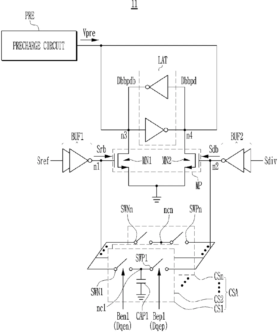
Samsung describes a digital phase lock loop circuit that uses a specific method to correct quantization noise, which is a type of error that occurs when converting analog signals to digital. The system adds a delay to one of the signals being compared based on correction codes to ensure the final output signal is more accurate.
In the filing’s own words
A digital phase lock loop circuit includes a phase detector to: receive a first reference signal and a first divided signal, selectively perform a delay operation on one of a second reference signal corresponding to the first reference signal and a second divided signal corresponding to the first divided signal, based on a first quantization noise correction code and a second quantization noise correction code, and output a phase difference code based on a phase difference between the second reference signal and the second divided signal on either of which the delay operation is performed; a digital loop filter to filter the phase difference code; an oscillator to generate an output signal based on the filtered phase difference code; a delta-sigma modulator to output a quantization noise signal and a division control signal based on first division ratio data and second division ratio data for the output signal.
What exactly they claim (claim 1)
1. A digital phase lock loop circuit comprising: a phase detector configured to: receive a first reference signal and a first divided signal, selectively perform a delay operation on one of a second reference signal corresponding to the first reference signal and a second divided signal corresponding to the first divided signal, based on a first quantization noise correction code and a second quantization noise correction code, and output a phase difference code based on a phase difference between the second reference signal and the second divided signal on either of which the delay operation is performed; a digital loop filter configured to filter the phase difference code; an oscillator configured to generate an output signal based on the filtered phase difference code; a delta-sigma modulator configured to output a quantization noise signal and a division control signal based on first division ratio data and second division ratio data for the output signal; an accumulation circuit configured to output a quantization noise code by performing an accumulation operation on the quantization noise signal; a divider configured to output the first divided signal by dividing a frequency of the output signal based on the division control signal; and a correction circuit configured to: generate the first quantization noise correction code and the second quantization noise correction code by performing a correction operation on the quantization noise code, and provide the first quantization noise correction code and the second quantization noise correction code to the phase detector.
Facts
- Company
- Samsung (Samsung Electronics Co., Ltd.)
- Official title
- DIGITAL PHASE LOCK LOOP AND METHOD OF OPERATING THE SAME
- Publication number
- US20260332151A1
- Application number
- 19569666
- Filed
- Mar 17, 2026
- Published
- Oct 22, 2026
- Inventors
- 3
- Claims
- 23
Classified under
H03L 7/0818 Electricity & electronicsH03L 7/089 Electricity & electronicsH03M 3/344 Electricity & electronicsMore from Samsung in Chips & hardware
- Samsung patents chip that combines camera and screen Oct 13, 2026
- Samsung patents faster chip testing using machine learning Sep 1, 2026
- Samsung patents radar method to pinpoint target direction more accurately Sep 1, 2026
- Samsung patents memory chip that searches data by content, not address Sep 1, 2026
- Samsung patents chip design that skips empty data to speed up AI Sep 1, 2026
Summaries are simplified from the filing’s own abstract and first claim. A patent filing is not a product announcement.
Patent data and drawings: U.S. Patent and Trademark Office (USPTO). Nebula is not affiliated with or endorsed by the USPTO.