Samsung patents memory chip that fixes errors from heavy use
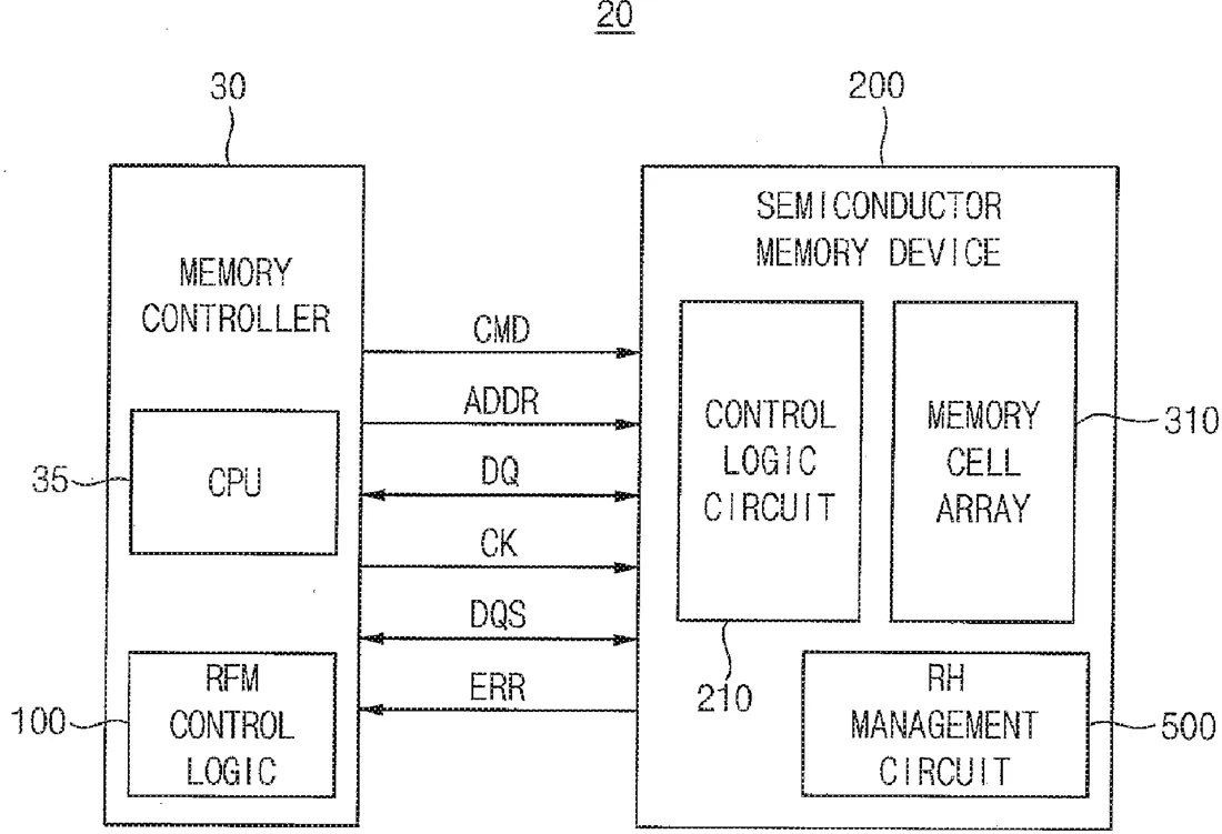
Samsung describes a memory device that tracks how often specific rows of data are accessed to prevent errors. When a row is accessed too frequently, the chip signals the system to pause and refresh nearby data rows to keep information safe.
In the filing’s own words
A semiconductor memory device includes a row hammer management circuit and a refresh control circuit. The row hammer management circuit counts the number of times of access on each memory cell row to store the counted values in count cells of each memory cell row as count data. A hammer address queue in the row hammer management circuit stores candidate hammer addresses, which are intensively accessed, in response to a number of the candidate hammer addresses reaching a second number, transitions a logic level of an error signal provided to the memory controller, and, in response to the number of the candidate hammer addresses reaching the first number, outputs one of the candidate hammer addresses as a hammer address. The refresh control circuit performs a hammer refresh operation on victim memory cell rows which are physically adjacent to a memory cell row corresponding to the hammer address.
What exactly they claim (claim 1)
1. A semiconductor memory device comprising: a memory cell array comprising a plurality of memory cell rows, wherein a target memory cell row of the plurality of memory cell rows includes one or more count cells configured to store count data indicating a number of accesses to the target memory cell row; an alert pin configured to transmit an alert signal; a row hammer management circuit configured to: perform an internal read-update-write operation on the target memory cell row among the plurality of memory cell rows in response to an active command; update the count data of the target memory cell row; and transition a logic level of the alert signal from a first logic level to a second logic level based on a comparison of the updated count data with a first threshold value, the transition of the alert signal to the second logic level indicating an error state such that an application of a subsequent active command is withheld and a refresh management (RFM) command is received; and a refresh control circuit configured to perform a hammer refresh operation on one or more victim memory cell rows among the plurality of memory cell rows in response to the RFM command, the one or more victim memory cell rows being physically adjacent to the target memory cell row, wherein the row hammer management circuit is configured to transition the logic level of the alert signal from the second logic level to the first logic level in response to a completion of the hammer refresh operation.
Facts
- Company
- Samsung (SAMSUNG ELECTRONICS CO., LTD.)
- Official title
- SEMICONDUCTOR MEMORY DEVICE AND MEMORY SYSTEM INCLUDING THE SAME
- Publication number
- US20260331158A1
- Application number
- 19727674
- Filed
- Jul 1, 2026
- Published
- Oct 22, 2026
- Inventors
- 1
- Claims
- 1
Classified under
G11C 11/40618 Physics & computingG11C 11/40611 Physics & computingG11C 11/4096 Physics & computingMore from Samsung in Chips & hardware
- Samsung patents chip that combines camera and screen Oct 13, 2026
- Samsung patents faster chip testing using machine learning Sep 1, 2026
- Samsung patents radar method to pinpoint target direction more accurately Sep 1, 2026
- Samsung patents memory chip that searches data by content, not address Sep 1, 2026
- Samsung patents chip design that skips empty data to speed up AI Sep 1, 2026
Summaries are simplified from the filing’s own abstract and first claim. A patent filing is not a product announcement.
Patent data and drawings: U.S. Patent and Trademark Office (USPTO). Nebula is not affiliated with or endorsed by the USPTO.