Samsung patents memory chip using ferroelectric material for data storage
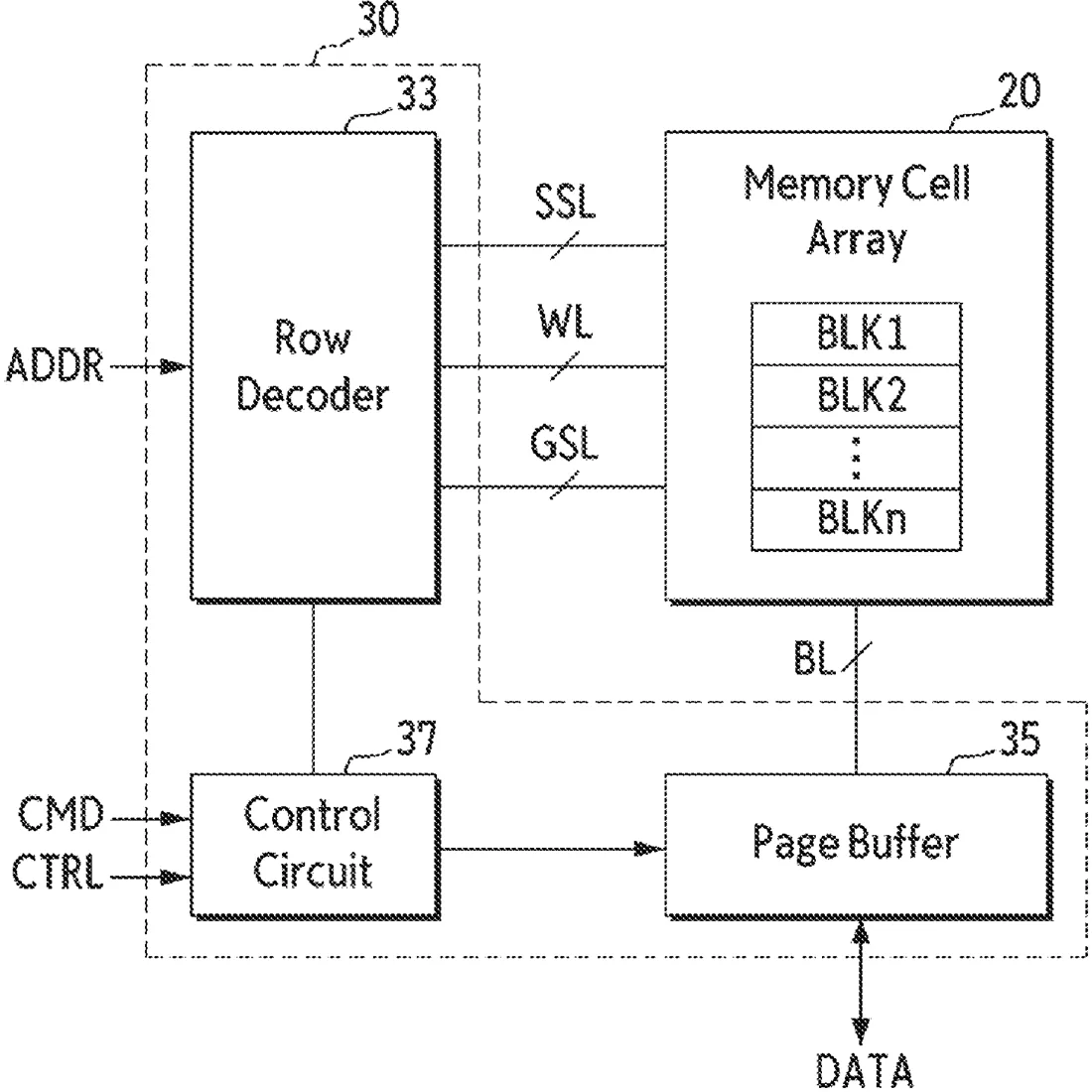
Samsung has filed a patent for a semiconductor memory device that uses a ferroelectric material to store data. The design places this storage material between word lines and a semiconductor pattern, with specific P-type materials used for the source line and channel pad to manage data flow.
In the filing’s own words
A semiconductor memory device including a ferroelectrics-based data storage element, a method for operating the same, and an electronic system including the same are provided. The semiconductor memory device includes a plurality of word lines spaced apart from each other in a first direction, a semiconductor pattern extending in the first direction and intersecting the plurality of word lines, a data storage pattern including a ferroelectric material, between the plurality of word lines and the semiconductor pattern, a common source line connected to the semiconductor pattern, under the plurality of word lines, a bit line on the plurality of word lines, and a channel pad connecting the semiconductor pattern and the bit line, wherein each of the common source line and the channel pad includes a P-type semiconductor material.
What exactly they claim (claim 1)
1. A semiconductor memory device comprising: a plurality of word lines spaced apart from each other in a first direction; a semiconductor pattern extending in the first direction and intersecting the plurality of word lines; a data storage pattern between the plurality of word lines and the semiconductor pattern, wherein the data storage pattern includes a ferroelectric material; a common source line under the plurality of word lines and connected to the semiconductor pattern; a bit line on the plurality of word lines; and a channel pad through which the semiconductor pattern and the bit line are connected to each other, wherein each of the common source line and the channel pad includes a P-type semiconductor material.
Facts
- Company
- Samsung (Samsung Electronics Co., Ltd.)
- Official title
- SEMICONDUCTOR MEMORY DEVICE, METHOD FOR OPERATING THE SAME AND ELECTRONIC SYSTEM INCLUDING THE SAME
- Publication number
- US20260331155A1
- Application number
- 19337125
- Filed
- Sep 23, 2025
- Published
- Oct 22, 2026
- Inventors
- 4
- Claims
- 20
Classified under
G11C 11/2257 Physics & computingG11C 11/2273 Physics & computingG11C 11/2275 Physics & computingMore from Samsung in Chips & hardware
- Samsung patents chip that combines camera and screen Oct 13, 2026
- Samsung patents faster chip testing using machine learning Sep 1, 2026
- Samsung patents radar method to pinpoint target direction more accurately Sep 1, 2026
- Samsung patents memory chip that searches data by content, not address Sep 1, 2026
- Samsung patents chip design that skips empty data to speed up AI Sep 1, 2026
Summaries are simplified from the filing’s own abstract and first claim. A patent filing is not a product announcement.
Patent data and drawings: U.S. Patent and Trademark Office (USPTO). Nebula is not affiliated with or endorsed by the USPTO.