Samsung patents display circuit that splits screen data into three timed groups
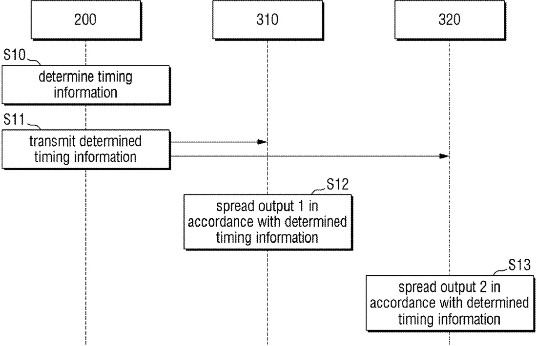
Samsung describes a display driving circuit that divides screen data into three separate groups, each sent through its own set of lines. The system uses feedback signals to ensure these three groups are sent at different times so they do not overlap.
In the filing’s own words
A display driving circuit is provided. The display driving circuit includes a timing controller configured to output image data and a source control signal, a first source driver circuit configured to output first source data of the image data by activating a plurality of first data lines in accordance with the source control signal, the first data lines having a first output spreading time, a second source driver circuit configured to output second source data of the image data by activating a plurality of second data lines in accordance with the source control signal, the second data lines having a second output spreading time, and a third source driver circuit configured to output third source data of the image data by activating a plurality of third data lines in accordance with the source control signal, the third data lines having a third output spreading time, wherein the first output spreading time, the second output spreading time and the third output spreading time do not overlap.
What exactly they claim (claim 1)
1. A display driving circuit comprising: a timing controller configured to output and randomly activate a first source control signal, a second source control signal and a third source control signal based on a main clock; a first source driver circuit connected to a plurality of first data lines of a display panel, configured to output a first source data through the plurality of first data lines based on the first source control signal and output a first feedback signal; a second source driver circuit connected to a plurality of second data lines of the display panel, configured to output a second source data through the plurality of second data lines based on the second source control signal and output a second feedback signal; a third source driver circuit connected to a plurality of third data lines of the display panel, configured to output a third source data through the plurality of third data lines based on the third source control signal and output a third feedback signal; wherein the timing controller determines first output spreading time of the plurality of first data lines based on the first feedback signal, second output spreading time of the plurality of second data lines based on the second feedback signal and third output spreading time of the plurality of third data lines based on the third feedback signal, wherein the first output spreading time, the second output spreading time and the third output spreading time are different from one another.
Facts
- Company
- Samsung (Samsung Electronics Co., Ltd.)
- Official title
- DISPLAY DRIVING CIRCUIT AND DISPLAY DEVICE THEREOF
- Publication number
- US20260331026A1
- Application number
- 19725472
- Filed
- Jun 30, 2026
- Published
- Oct 22, 2026
- Inventors
- 6
- Claims
- 20
Classified under
G09G 3/2096 Physics & computingG09G 3/3275 Physics & computingG09G 3/3685 Physics & computingG09G 2310/08 Physics & computingG09G 2330/06 Physics & computingMore from Samsung in Chips & hardware
- Samsung patents chip that combines camera and screen Oct 13, 2026
- Samsung patents faster chip testing using machine learning Sep 1, 2026
- Samsung patents radar method to pinpoint target direction more accurately Sep 1, 2026
- Samsung patents memory chip that searches data by content, not address Sep 1, 2026
- Samsung patents chip design that skips empty data to speed up AI Sep 1, 2026
Summaries are simplified from the filing’s own abstract and first claim. A patent filing is not a product announcement.
Patent data and drawings: U.S. Patent and Trademark Office (USPTO). Nebula is not affiliated with or endorsed by the USPTO.