Samsung patents memory chip that sorts AI tasks by workload
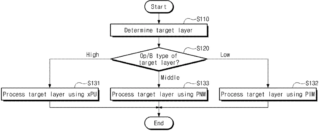
Samsung describes a memory device that handles different parts of an AI model based on how much math each part requires. It sends heavy calculations to an external processor, medium ones to a nearby unit, and light ones directly inside the memory.
In the filing’s own words
A heterogeneous computation memory device includes a memory including a processing-in-memory (PIM), a processing-near-memory (PNM) unit, and a controller configured to receive first to third requests from a processing device via a host channel, and to control the memory and the PNM unit via the memory channel. The first request corresponds to a first layer having a first computational intensity, the second request corresponds to a second layer having a second computational intensity, and the third request corresponds to a third layer having a third computational intensity. The controller transmits first target data stored in the memory to the external computation unit in response to the first request, controls the PNM unit to process the second layer in response to the second request, and controls the memory to process the third layer in response to the third request.
What exactly they claim (claim 1)
1. A heterogeneous computing memory device comprising: a memory including a processing-in-memory (PIM) unit; a processing-near-memory (PNM) unit; and a controller configured to receive first to third requests from an external processing device via a host channel and configured to, in response to the first to third requests, control the memory and the PNM unit via a memory channel, wherein the first request corresponds to a first layer having a first computational intensity, the second request corresponds to a second layer having a second computational intensity lower than the first computational intensity, and the third request corresponds to a third layer having a third computational intensity lower than the second computational intensity, and wherein the controller is configured to: in response to the first request, provide first target data stored in the memory to the external processing device; in response to the second request, control the PNM unit to process the second layer by the PNM unit; and in response to the third request, control the memory to process the third layer by the PIM unit of the memory.
Facts
- Company
- Samsung (Samsung Electronics Co., Ltd.)
- Official title
- HETEROGENEOUS COMPUTING MEMORY DEVICE AND ARTIFICIAL INTELLIGENCE COMPUTING SYSTEM INCLUDING THE SAME
- Publication number
- US20260330207A1
- Application number
- 19446433
- Filed
- Jan 12, 2026
- Published
- Oct 22, 2026
- Inventors
- 7
- Claims
- 20
Classified under
G06N 3/063 Physics & computingG06F 13/4031 Physics & computingG06N 3/045 Physics & computingG06F 2213/0026 Physics & computingMore from Samsung in Chips & hardware
- Samsung patents chip that combines camera and screen Oct 13, 2026
- Samsung patents faster chip testing using machine learning Sep 1, 2026
- Samsung patents radar method to pinpoint target direction more accurately Sep 1, 2026
- Samsung patents memory chip that searches data by content, not address Sep 1, 2026
- Samsung patents chip design that skips empty data to speed up AI Sep 1, 2026
Summaries are simplified from the filing’s own abstract and first claim. A patent filing is not a product announcement.
Patent data and drawings: U.S. Patent and Trademark Office (USPTO). Nebula is not affiliated with or endorsed by the USPTO.