Google patents chip design trick to speed up testing
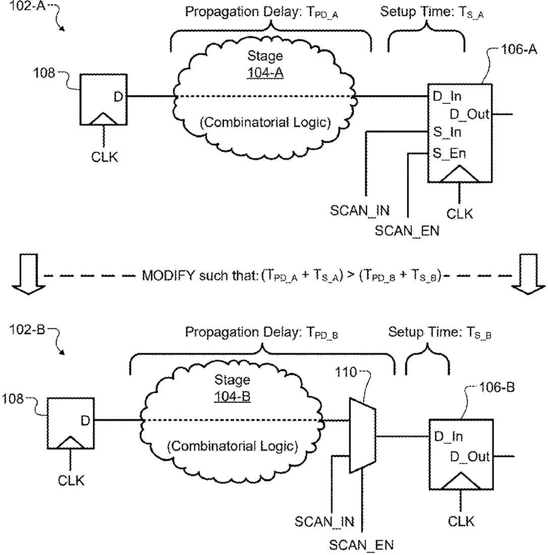
Google describes a method for designing digital circuits that mixes standard and special memory components. It automatically replaces certain memory parts with simpler versions when the logic before them is slow, while keeping others standard to maintain testability.
In the filing’s own words
Implementations described herein relate to non-scannable flip-flops used within scannable digital circuits. For example, an illustrative method includes determining that a first propagation delay of a first stage of combinatorial logic is greater than a delay threshold, the first stage preceding a first scannable flip-flop within a scannable digital circuit design, and, based on that determination, modifying the scannable digital circuit design to integrate a multiplexing function controlled by a scan enable signal into the first stage and to convert the first scannable flip-flop into a non-scannable flip-flop. The method further includes determining that a second propagation delay of a second stage of combinatorial logic is less than the delay threshold, the second stage preceding a second scannable flip-flop within the scannable digital circuit design, and, based on that determination, retaining the second scannable flip-flop in the circuit design. Corresponding methods, circuits, media, and other implementations are also disclosed.
What exactly they claim (claim 1)
1. A scannable digital circuit comprising: a first stage of combinatorial logic configured to perform, at an output of the first stage, a multiplexing function controlled by a scan enable signal; a first flip-flop configured to receive the output of the first stage after the multiplexing function is performed, the first flip-flop being a non-scannable flip-flop; a second stage of combinatorial logic; and a second flip-flop configured to receive an output of the second stage, the second flip-flop being a scannable flip-flop that is configured to perform the multiplexing function controlled by the scan enable signal.
Facts
- Company
- Google (Google LLC)
- Official title
- NON-SCANNABLE FLIP-FLOP FOR A SCANNABLE DIGITAL CIRCUIT
- Publication number
- US20260330115A1
- Application number
- 19186319
- Filed
- Apr 22, 2025
- Published
- Oct 22, 2026
- Inventors
- 2
- Claims
- 20
Classified under
G06F 30/3312 Physics & computingG06F 2119/12 Physics & computingMore from Google in Chips & hardware
- Google patents quantum gates to simulate particle physics Sep 1, 2026
- Waymo patents lidar chips that split light into multiple beams Sep 8, 2026
- Google patents chip design to speed up AI math tasks Sep 8, 2026
- Google patents display that turns off colors to save battery Sep 8, 2026
- Google patents display tech that skips blank screen areas to save power Sep 15, 2026
Summaries are simplified from the filing’s own abstract and first claim. A patent filing is not a product announcement.
Patent data and drawings: U.S. Patent and Trademark Office (USPTO). Nebula is not affiliated with or endorsed by the USPTO.