Samsung patents processor self-test using weighted scan chains
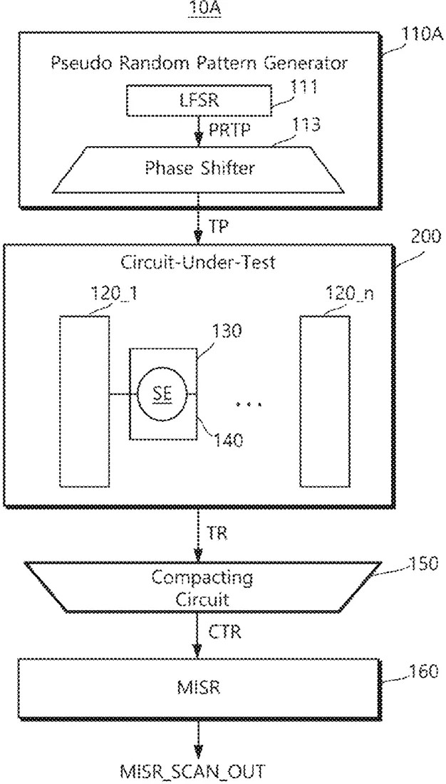
Samsung describes a processor design that includes built-in circuits to automatically check for manufacturing defects. It uses a method called scan testing, where test patterns are pushed through the chip's logic, and specific signals are weighted or controlled to create a final signature that indicates if the chip is working correctly.
In the filing’s own words
A processor includes a pattern generating circuit configured to output a test pattern of pseudo-random numbers, a plurality of scan chains, each including a plurality of scan cells connected in a chain, configured to scan-in the test pattern to the plurality of scan cells and scan-out a response of a circuit-under-test based on the test pattern, the circuit-under-test comprising logic circuits coupled to the plurality of scan cells, a weight applying circuit configured to apply a weight to an output signal of at least one scan cell among the plurality of scan cells, a control point circuit configured to share at least one element with the weight applying circuit, and a compacting circuit configured to output a signature obtained by compacting a test response of the circuit-under-test.
What exactly they claim (claim 1)
1. A processor, comprising: a pattern generating circuit configured to transmit a test pattern of pseudo-random numbers; a scan chain, the scan chain including a plurality of scan cells connected in a chain, the scan chain configured to scan-in the test pattern to the plurality of scan cells and scan-out a test response of a circuit-under-test based on the test pattern, the plurality of scan cells coupled to at least one logic circuit of the circuit-under-test; a weight applying circuit and a control point circuit, the weight applying circuit and the control point circuit configured to share at least one shared element, the weight applying circuit configured to transmit a weighted output signal to the circuit-under-test by applying a weight to an output signal of at least one scan cell among the plurality of scan cells based on an operation performed by the at least one shared element, the control point circuit configured to selectively control blocking of an internal signal of the circuit-under-test and transmitting a pre-configured logic value to the circuit-under-test or transmitting the internal signal to the circuit-under-test without blocking, such that one of the pre-configured logic value or the internal signal is transmitted to the circuit-under-test based on the operation performed by the at least one shared element; and a compacting circuit configured to transmit a signature obtained based on compacting the test response of the circuit-under-test.
Facts
- Company
- Samsung (Samsung Electronics Co., Ltd.)
- Official title
- PROCESSOR INCLUDING BUILT-IN SELF-TEST CIRCUIT, METHOD OF OPERATING THE PROCESSOR, AND METHOD OF MANUFACTURING THE SAME
- Publication number
- US20260329710A1
- Application number
- 19644433
- Filed
- Apr 10, 2026
- Published
- Oct 22, 2026
- Inventors
- 2
- Claims
- 20
Classified under
G06F 11/2284 Physics & computingG06F 11/263 Physics & computingMore from Samsung in Chips & hardware
- Samsung patents chip that combines camera and screen Oct 13, 2026
- Samsung patents faster chip testing using machine learning Sep 1, 2026
- Samsung patents radar method to pinpoint target direction more accurately Sep 1, 2026
- Samsung patents memory chip that searches data by content, not address Sep 1, 2026
- Samsung patents chip design that skips empty data to speed up AI Sep 1, 2026
Summaries are simplified from the filing’s own abstract and first claim. A patent filing is not a product announcement.
Patent data and drawings: U.S. Patent and Trademark Office (USPTO). Nebula is not affiliated with or endorsed by the USPTO.