Samsung patents chip management system that balances power and wear across dies
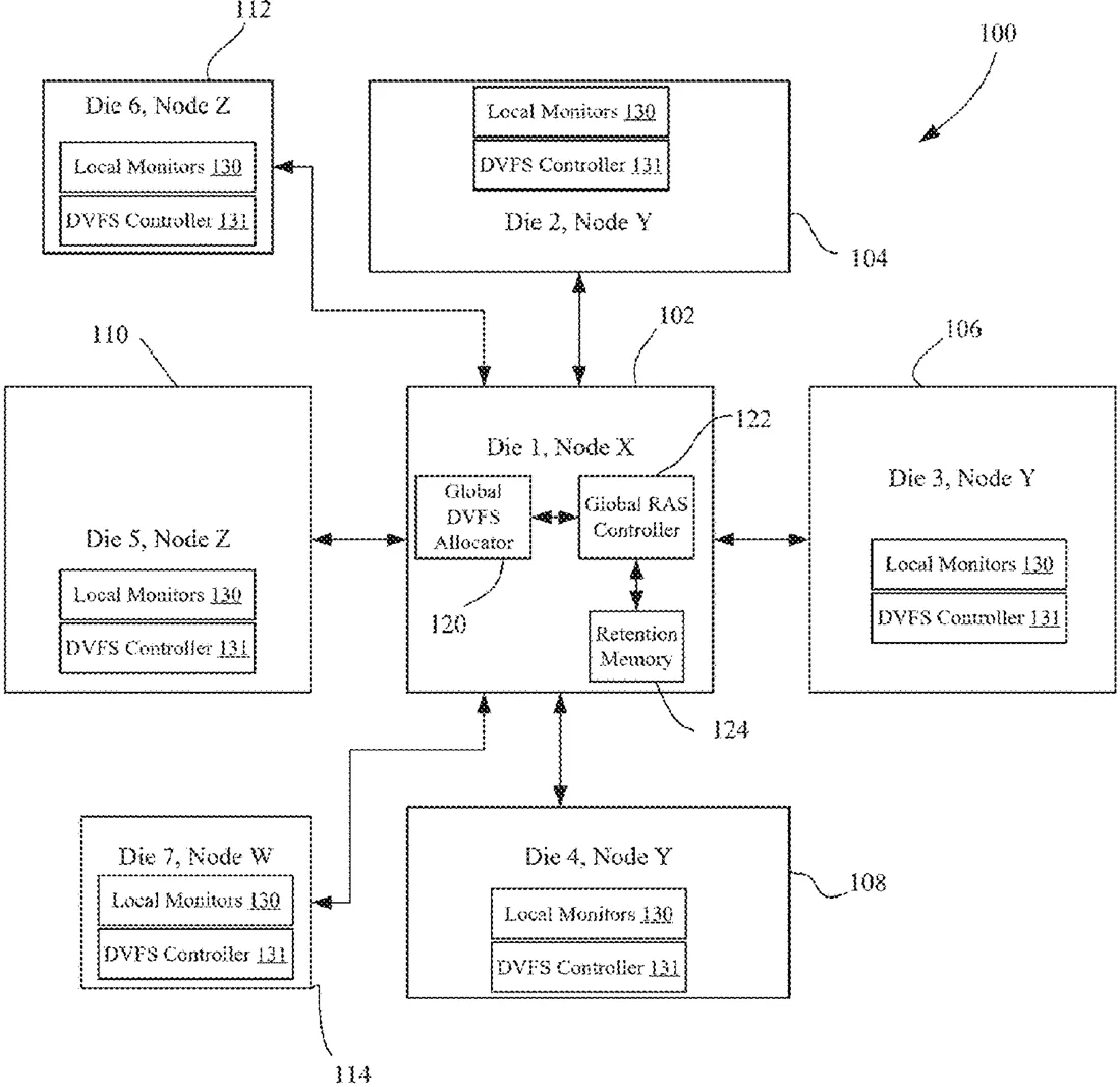
Samsung describes a system for managing power and performance in advanced chips made of multiple smaller parts called chiplets. A central controller collects data on temperature and workload from each part, then adjusts power usage to balance performance and prevent one part from wearing out faster than the others.
In the filing’s own words
A method and system for managing dynamic voltage/frequency scaling (DVFS) and aging in chiplet-based system on integrated circuit (SoIC) architectures are disclosed. The method involves resetting multiple dies upon power-up, each equipped with local DVFS controllers and monitors to measure operating parameters such as voltage, temperature, and workload indicators. A global DVFS allocator receives performance data from the local monitors, adjusts DVFS credit allocations based on a calibrated global DVFS policy, and communicates power shifting instructions to the local controllers. Aging uniformity is managed by a global reliability, availability, and serviceability (RAS) controller, which retrieves historical aging data from retention memory and applies adjustments to optimize system reliability. The system includes a global DVFS allocator, a global RAS controller, and retention memory for storing operational parameters and aging data. This approach enhances performance, reliability, and resource allocation in semiconductor technologies, particularly for SoIC architectures.
What exactly they claim (claim 1)
1. A method for managing dynamic voltage/frequency scaling (DVFS) and aging in a chiplet-based system on integrated circuit (SoIC) architecture, comprising: resetting, upon power-up, a plurality of dies in the SoIC, each die including a local DVFS controller and local monitors configured to measure voltage, temperature, frequency, speed, leakage, and workload indicators; receiving, at a global DVFS allocator, performance data from the local monitors of each die, the performance data including front-end performance counters and back-end loading indicators; adjusting, by the global DVFS allocator, DVFS credit allocations for the dies based on a calibrated global DVFS policy derived from the received performance data; communicating, from the global DVFS allocator, power shifting instructions to the local DVFS controllers associated with the dies; and retrieving historical aging data of each die of the plurality of dies stored in a retention memory and applying, by a global RAS controller operating in cooperation with the global DVFS allocator, aging adjustments to each of the local DVFS controllers across the SoIC.
Facts
- Company
- Samsung (Samsung Electronics Co., Ltd.)
- Official title
- GLOBAL RAS DECISION AND DVFS ALLOCATOR WITH PER DIE MONITORS AND CONTROLLERS IN CHIPLET ARCHITECTURES
- Publication number
- US20260329452A1
- Application number
- 19313476
- Filed
- Aug 28, 2025
- Published
- Oct 22, 2026
- Inventors
- 1
- Claims
- 23
Classified under
G06F 3/0616 Physics & computingG06F 3/0634 Physics & computingG06F 3/0679 Physics & computingG06F 9/5066 Physics & computingG06F 2209/501 Physics & computingMore from Samsung in Chips & hardware
- Samsung patents chip that combines camera and screen Oct 13, 2026
- Samsung patents faster chip testing using machine learning Sep 1, 2026
- Samsung patents radar method to pinpoint target direction more accurately Sep 1, 2026
- Samsung patents memory chip that searches data by content, not address Sep 1, 2026
- Samsung patents chip design that skips empty data to speed up AI Sep 1, 2026
Summaries are simplified from the filing’s own abstract and first claim. A patent filing is not a product announcement.
Patent data and drawings: U.S. Patent and Trademark Office (USPTO). Nebula is not affiliated with or endorsed by the USPTO.