Samsung patents display assembly using notched adhesive strips
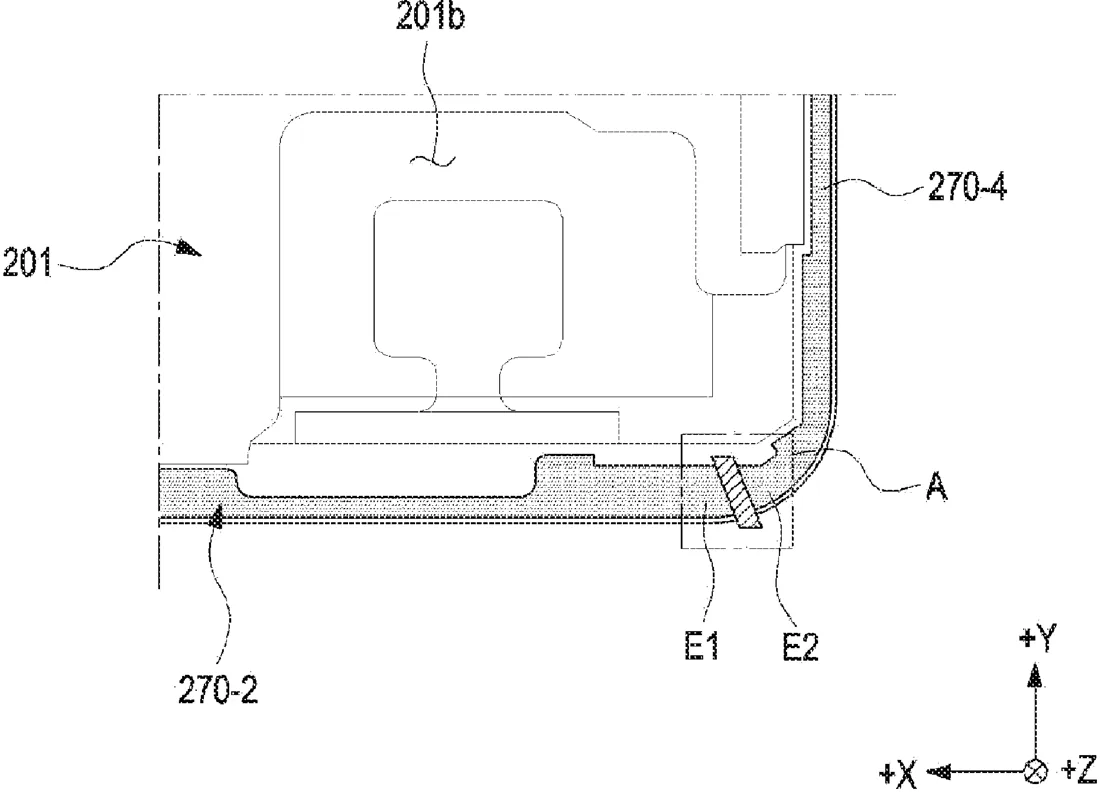
Samsung describes a method for attaching a screen to a device frame using multiple small adhesive strips instead of one continuous piece. The ends of these strips are cut with notches to create specific gaps where additional adhesive material is applied to secure the display.
In the filing’s own words
An electronic device is provided. The electronic device includes a housing forming an exterior of the electronic device, the housing including a support structure, a display disposed at the housing, the display including a first surface facing the support structure, a plurality of adhesive members disposed on the first surface of the display along an edge of the display, the plurality of adhesive members being spaced apart from each other, and an adhesive material, wherein each of one or more separation areas is defined between a first end portion of one of the plurality of adhesive members and a second end portion of another of the plurality of adhesive members adjacent thereto, wherein each of the one or more separation areas includes an application area in which the adhesive material is disposed, wherein at least one of the first end portion or the second end portion includes a cut portion having a notch shape, thereby forming the application area, and extension areas connected to a first side of the application area and a second side of the application area opposite to the first side, respectively, wherein the extension areas are defined by a portion of the first end portion and a portion of the second end portion.
What exactly they claim (claim 1)
1. An electronic device comprising: a housing forming an exterior of the electronic device, the housing including a support structure; a display disposed at the housing, the display including an first surface facing the support structure; a plurality of adhesive members disposed on the first surface of the display along an edge of the display, the plurality of adhesive members being spaced apart from each other; and an adhesive material, wherein each of one or more separation areas is defined between a first end portion of one of the plurality of adhesive members and a second end portion of another of the plurality of adhesive members adjacent thereto, the second end portion facing the first end portion, wherein each of the one or more separation areas includes: an application area in which the adhesive material is disposed, wherein at least one of the first end portion or the second end portion includes a cut portion having a notch shape, thereby forming the application area; and extension areas connected to a first side of the application area and a second side of the application area opposite to the first side, respectively, wherein the extension areas are defined by a portion of the first end portion and a portion of the second end portion.
Facts
- Company
- Samsung (Samsung Electronics Co., Ltd.)
- Official title
- ELECTRONIC DEVICE COMPRISING DISPLAY
- Publication number
- US20260329349A1
- Application number
- 19692186
- Filed
- May 29, 2026
- Published
- Oct 22, 2026
- Inventors
- 2
- Claims
- 20
Classified under
G06F 1/1656 Physics & computingH04M 1/0249 Electricity & electronicsH04M 1/0266 Electricity & electronicsH05K 5/064 Electricity & electronicsMore from Samsung in Chips & hardware
- Samsung patents chip that combines camera and screen Oct 13, 2026
- Samsung patents faster chip testing using machine learning Sep 1, 2026
- Samsung patents radar method to pinpoint target direction more accurately Sep 1, 2026
- Samsung patents memory chip that searches data by content, not address Sep 1, 2026
- Samsung patents chip design that skips empty data to speed up AI Sep 1, 2026
Summaries are simplified from the filing’s own abstract and first claim. A patent filing is not a product announcement.
Patent data and drawings: U.S. Patent and Trademark Office (USPTO). Nebula is not affiliated with or endorsed by the USPTO.