Samsung patents method for making display light sources with solder bridges
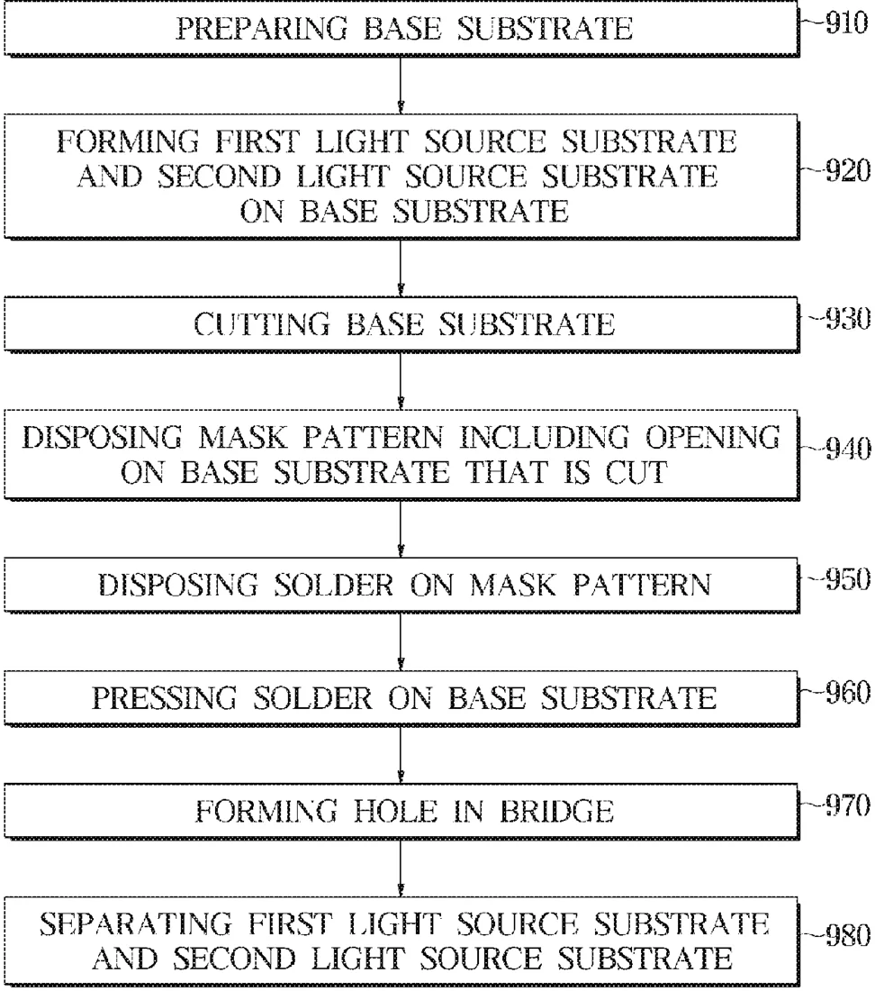
Samsung describes a manufacturing process for a light source device used in displays. The method involves creating two substrate layers with alternating bars, connecting them with bridges, and using a mask to guide solder into specific openings to secure the components.
In the filing’s own words
There is provided a method for manufacturing a light source device including a first light source substrate and a second light source substrate, the method including: forming, in a base substrate, the first light source substrate including a first substrate body, extending in a first direction, and a first substrate bar extending from the first substrate body in a second direction; forming, in the base substrate, the second light source substrate including a second substrate body, extending in the first direction, and a second substrate bar extending from the second substrate body in a third direction opposite to the second direction and disposed alternately with the first substrate bar; forming bridges connecting the first light source substrate and the second light source substrate; disposing, on the base substrate, a mask pattern including an opening; disposing a solder on the mask pattern; and introducing the solder into the opening.
What exactly they claim (claim 1)
1. A method for manufacturing a light source device comprising a first light source substrate and a second light source substrate, the method comprising: forming, in a base substrate, the first light source substrate comprising a first substrate body, extending in a first direction, and a first substrate bar extending from the first substrate body in a second direction; forming, in the base substrate, the second light source substrate comprising a second substrate body, extending in the first direction, and a second substrate bar extending from the second substrate body in a third direction opposite to the second direction and disposed alternately with the first substrate bar; forming, by a cutting of the base substrate, a plurality of bridges connecting the first light source substrate and the second light source substrate, the first substrate body of the first light source substrate and one end of the second substrate bar of the second light source substrate in the third direction are connected by the plurality of bridges; disposing, on the base substrate and after the cutting the base substrate, a mask pattern comprising an opening; disposing a solder on the mask pattern; and introducing, by a pressing of the solder on the mask pattern, the solder into the opening.
Facts
- Company
- Samsung (SAMSUNG ELECTRONICS CO., LTD.)
- Official title
- LIGHT SOURCE DEVICE, METHOD FOR MANUFACTURING SAME, AND DISPLAY APPARATUS COMPRISING LIGHT SOURCE DEVICE
- Publication number
- US20260329129A1
- Application number
- 19692761
- Filed
- May 29, 2026
- Published
- Oct 22, 2026
- Inventors
- 5
- Claims
- 12
Classified under
G02F 1/133603 Physics & computingB23K 1/0016 Operations & transportB23K 2101/36 Operations & transportMore from Samsung in Chips & hardware
- Samsung patents chip that combines camera and screen Oct 13, 2026
- Samsung patents faster chip testing using machine learning Sep 1, 2026
- Samsung patents radar method to pinpoint target direction more accurately Sep 1, 2026
- Samsung patents memory chip that searches data by content, not address Sep 1, 2026
- Samsung patents chip design that skips empty data to speed up AI Sep 1, 2026
Summaries are simplified from the filing’s own abstract and first claim. A patent filing is not a product announcement.
Patent data and drawings: U.S. Patent and Trademark Office (USPTO). Nebula is not affiliated with or endorsed by the USPTO.