Samsung patents processor with built-in self-test circuit
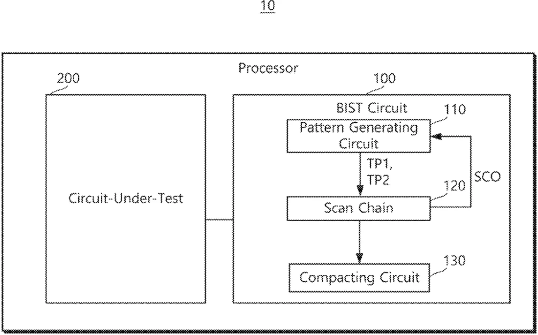
Samsung describes a processor design that includes a built-in system to check for manufacturing defects. It uses a chain of storage cells to send specific test signals through the chip's logic and compares the results to a pre-set signature to verify the hardware is working correctly.
In the filing’s own words
A processor includes a scan chain including a plurality of scan cells connected in a chain, the scan chain configured to scan-in an input signal sequentially to the plurality of scan cells, store the input signal as a test pattern, and scan-out a test response from a circuit-under-test based on the test pattern, a pattern generating circuit generates a first test pattern based on a pseudo-random pattern, a second test pattern based on a deterministic pattern, and transmits the first test pattern and the second test pattern to the scan chain, the circuit-under-test comprises a logic circuit coupled to the plurality of scan cells, and a compacting circuit configured to output a signature by compacting the test response of the circuit-under-test. The pattern generating circuit generates a portion of the first and second test pattern based on an output signal of one scan cell of the plurality of scan cells.
What exactly they claim (claim 1)
1. A processor comprising: a scan chain including a plurality of scan cells connected in a chain, the scan chain configured to scan-in an input signal sequentially to the plurality of scan cells, store the input signal as a test pattern, and scan-out a test response from a circuit-under-test based on the test pattern; a pattern generating circuit configured to generate a first test pattern based on a pseudo-random pattern, generate a second test pattern based on a deterministic pattern, and transmit the first test pattern and the second test pattern to the scan chain; the circuit-under-test comprising a logic circuit coupled to the plurality of scan cells; and a compacting circuit configured to output a signature by compacting the test response of the circuit-under-test, wherein the pattern generating circuit is further configured to generate at least a portion of the first test pattern and the second test pattern based on an output signal of at least one scan cell of the plurality of scan cells.
Facts
- Company
- Samsung (Samsung Electronics Co., Ltd.)
- Official title
- PROCESSOR INCLUDING BUILT-IN SELF-TEST CIRCUIT, METHOD OF OPERATING THE PROCESSOR, AND METHOD OF MANUFACTURING THE SAME
- Publication number
- US20260328843A1
- Application number
- 19647095
- Filed
- Apr 14, 2026
- Published
- Oct 22, 2026
- Inventors
- 2
- Claims
- 20
Classified under
G01R 31/318547 Physics & computingG01R 31/318385 Physics & computingG01R 31/31921 Physics & computingG01R 31/318536 Physics & computingMore from Samsung in Chips & hardware
- Samsung patents chip that combines camera and screen Oct 13, 2026
- Samsung patents faster chip testing using machine learning Sep 1, 2026
- Samsung patents radar method to pinpoint target direction more accurately Sep 1, 2026
- Samsung patents memory chip that searches data by content, not address Sep 1, 2026
- Samsung patents chip design that skips empty data to speed up AI Sep 1, 2026
Summaries are simplified from the filing’s own abstract and first claim. A patent filing is not a product announcement.
Patent data and drawings: U.S. Patent and Trademark Office (USPTO). Nebula is not affiliated with or endorsed by the USPTO.