Samsung patents new circuit design to test chip components more efficiently
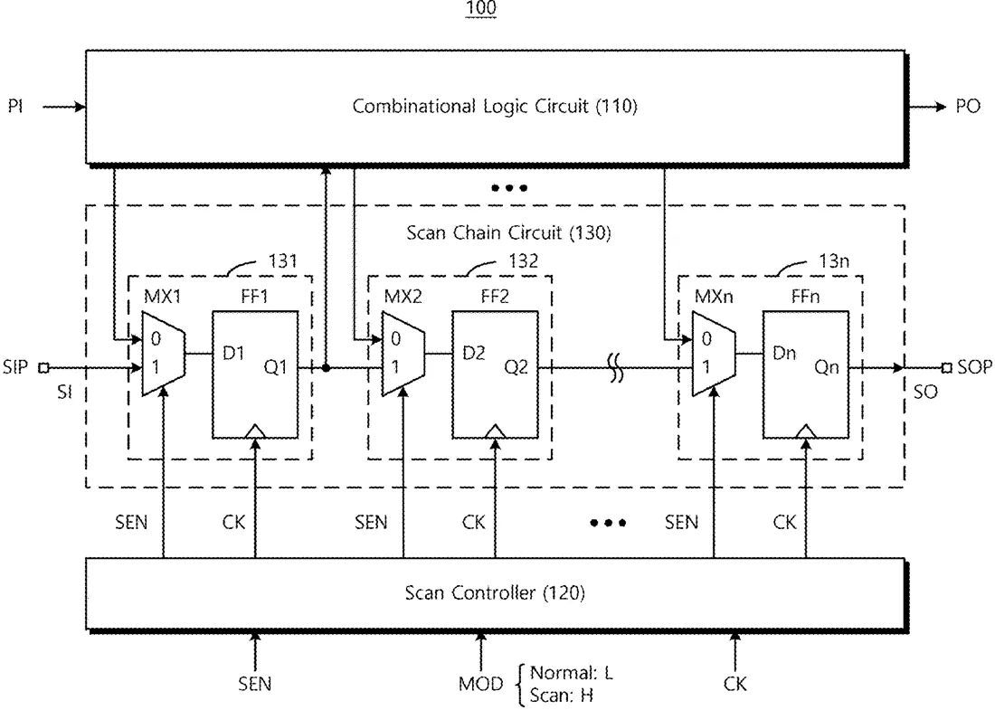
Samsung has filed a patent for a specific type of scan chain circuit used in semiconductor testing. The design uses two different latches to capture signals from logic circuits at different times, allowing engineers to check if the chip is working correctly. This method helps identify defects in the manufacturing process before the chip is sold.
In the filing’s own words
A scan chain circuit of a semiconductor integrated circuit includes a first scan latch and a second scan latch. The first scan latch is configured to receive a first signal from a combinational logic circuit during a first scan operation and store the first signal in a master latch in response to a first clock signal. The first scan latch is also configured to receive a second signal from the combinational logic circuit during a second scan operation and store the second signal in the master latch in response to the first clock signal. The second scan latch is configured to form a scan chain with the first scan latch, and store a signal provided from the combinational logic circuit in a slave latch in response to a second clock signal.
What exactly they claim (claim 1)
1. A scan chain circuit of a semiconductor integrated circuit, comprising: a first scan latch configured to receive a first signal from a combinational logic circuit during a first scan operation and store the first signal in a master latch in response to a first clock signal, and receive a second signal from the combinational logic circuit during a second scan operation and store the second signal in the master latch in response to the first clock signal; and a second scan latch configured to form a scan chain with the first scan latch, and store a signal provided from the combinational logic circuit in a slave latch in response to a second clock signal.
Facts
- Company
- Samsung (SAMSUNG ELECTRONICS CO., LTD.)
- Official title
- SCAN CHAIN CIRCUIT OF SEMICONDUCTOR INTEGRATED CIRCUIT AND SCAN TEST OPERATION METHOD THEREOF
- Publication number
- US20260328842A1
- Application number
- 19463682
- Filed
- Jan 29, 2026
- Published
- Oct 22, 2026
- Inventors
- 2
- Claims
- 20
Classified under
G01R 31/318536 Physics & computingG01R 31/318541 Physics & computingG01R 31/318555 Physics & computingG01R 31/318583 Physics & computingG01R 31/318594 Physics & computingMore from Samsung in Chips & hardware
- Samsung patents chip that combines camera and screen Oct 13, 2026
- Samsung patents faster chip testing using machine learning Sep 1, 2026
- Samsung patents radar method to pinpoint target direction more accurately Sep 1, 2026
- Samsung patents memory chip that searches data by content, not address Sep 1, 2026
- Samsung patents chip design that skips empty data to speed up AI Sep 1, 2026
Summaries are simplified from the filing’s own abstract and first claim. A patent filing is not a product announcement.
Patent data and drawings: U.S. Patent and Trademark Office (USPTO). Nebula is not affiliated with or endorsed by the USPTO.