Samsung patents laser method to cut chips faster
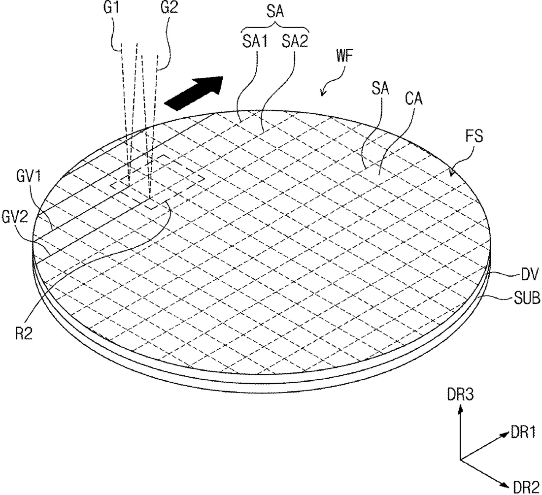
This filing describes a way to cut silicon wafers into individual chips using two laser beams. The method allows the lasers to work at the same time or separately, creating grooves in the wafer before it is sliced into final components.
In the filing’s own words
A method for manufacturing a semiconductor device includes preparing a wafer having chip regions and scribe lane regions that define the chip regions, the scribe lane regions including a first scribe lane region and a second scribe lane region that extend parallel to each other in a scan direction, forming a first groove by emitting a first beam to the first scribe lane region along the scan direction, forming a second groove by emitting a second beam to the second scribe lane region along the scan direction, attaching a dicing tape to a backside of the wafer, and cutting the wafer into semiconductor devices. The first beam and the second beam are simultaneously emitted during a dual emission period. One of the first beam and the second beam is blocked during a single emission period, and the other one is emitted during the single emission period.
What exactly they claim (claim 1)
1. A method for manufacturing a semiconductor device, the method comprising: preparing a wafer having a plurality of chip regions and a plurality of scribe lane regions defining the plurality of chip regions, wherein the plurality of scribe lane regions include a first scribe lane region and a second scribe lane region that extend parallel to each other in a scan direction; forming a plurality of grooves in at least one of a dual emission period or a single emission period; attaching a dicing tape to a backside of the wafer; and cutting the wafer into a plurality of semiconductor devices, wherein forming the plurality of grooves include: during the single emission period, forming a first groove of the plurality of grooves by emitting a first beam to the first scribe lane region along the scan direction, and forming a second groove of the plurality of grooves by independently emitting a second beam to the second scribe lane region along the scan direction, or during the dual emission period, forming the first groove and forming the second groove by simultaneously emitting the first beam and the second beam to the first scribe lane region and the second scribe lane region along the scan direction, respectively.
Facts
- Company
- Samsung (Samsung Electronics Co., Ltd.)
- Official title
- METHOD FOR MANUFACTURING SEMICONDUCTOR DEVICE INCLUDING DICING WAFER
- Publication number
- US20260324333A1
- Application number
- 19578362
- Filed
- Mar 25, 2026
- Published
- Oct 15, 2026
- Inventors
- 5
- Claims
- 20
Classified under
H10P 58/20 Electricity & electronicsH10P 34/42 Electricity & electronicsMore from Samsung in Chips & hardware
- Samsung patents chip that combines camera and screen Oct 13, 2026
- Samsung patents faster chip testing using machine learning Sep 1, 2026
- Samsung patents radar method to pinpoint target direction more accurately Sep 1, 2026
- Samsung patents memory chip that searches data by content, not address Sep 1, 2026
- Samsung patents chip design that skips empty data to speed up AI Sep 1, 2026
Summaries are simplified from the filing’s own abstract and first claim. A patent filing is not a product announcement.
Patent data and drawings: U.S. Patent and Trademark Office (USPTO). Nebula is not affiliated with or endorsed by the USPTO.