Samsung patents quantum chip design using junction shape to control resistance
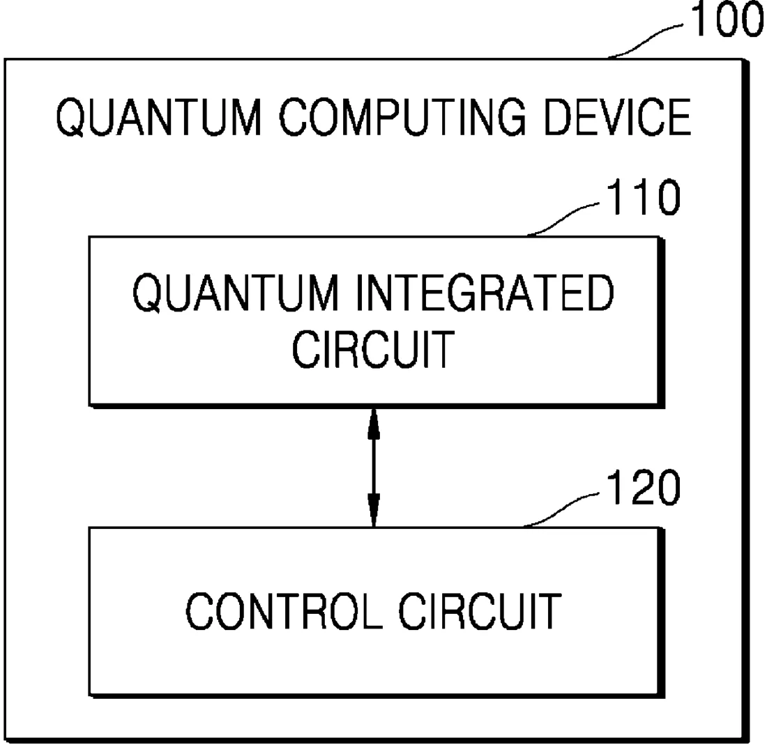
Samsung describes a quantum device built on a chip that uses a specific shape for its superconducting junctions. The invention adjusts the ratio between the junction's width and its step height to manage how electrical resistance varies across the component.
In the filing’s own words
Provided are a quantum apparatus and method. The quantum apparatus includes a first electrode layer that extends in a first direction on a substrate, a second electrode layer that extends in a second direction on the substrate, a Josephson junction formed by the second electrode layer overlapping the first electrode layer, and capacitor pads that form a resonance circuit with the Josephson junction, wherein the Josephson junction has a first length that is defined as a length of a top edge along which the second electrode layer extends across the first electrode layer in the second direction, and has a second length that is defined as a length of a step edge where the second electrode layer extends upward to overlap or be above the first electrode layer, and wherein a ratio of the first length to the second length corresponds to a resistance dispersion of the Josephson junction.
What exactly they claim (claim 1)
1. A quantum apparatus comprising: a first electrode layer that extends in a first direction on a substrate; a second electrode layer that extends in a second direction on the substrate; a Josephson junction formed by an overlapping of the first electrode layer by the second electrode layer; and capacitor pads that form a resonance circuit together with the Josephson junction, wherein the Josephson junction has a first length that is defined as a length of a top edge, of the Josephson junction, along which the second electrode layer extends across the first electrode layer in the second direction, and has a second length that is defined as a length of a step edge of the Josephson junction where the second electrode layer extends upward to overlap or be above the first electrode layer, and wherein a ratio of the first length to the second length corresponds to a resistance dispersion of the Josephson junction.
Facts
- Company
- Samsung (Samsung Electronics Co., Ltd.)
- Official title
- QUANTUM APPARATUS AND METHOD BASED ON A JOSEPHSON JUNCTION RESISTANCE DISPERSION
- Publication number
- US20260324298A1
- Application number
- 19465206
- Filed
- Jan 30, 2026
- Published
- Oct 15, 2026
- Inventors
- 6
- Claims
- 20
Classified under
H10N 60/12 Electricity & electronicsG06N 10/40 Physics & computingH10N 60/805 Electricity & electronicsH10N 60/82 Electricity & electronicsMore from Samsung in Chips & hardware
- Samsung patents chip that combines camera and screen Oct 13, 2026
- Samsung patents faster chip testing using machine learning Sep 1, 2026
- Samsung patents radar method to pinpoint target direction more accurately Sep 1, 2026
- Samsung patents memory chip that searches data by content, not address Sep 1, 2026
- Samsung patents chip design that skips empty data to speed up AI Sep 1, 2026
Summaries are simplified from the filing’s own abstract and first claim. A patent filing is not a product announcement.
Patent data and drawings: U.S. Patent and Trademark Office (USPTO). Nebula is not affiliated with or endorsed by the USPTO.