Samsung patents method to build MRAM memory with protective oxide layer
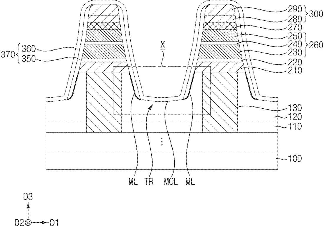
This filing describes a step-by-step process for creating magnetic random access memory (MRAM) chips. It details how to etch the memory structure to create a small trench and then use a chemical oxidation process to turn leftover metal into a protective oxide layer at the bottom of that trench.
In the filing’s own words
In a method of manufacturing an MRAM device, an MTJ layer structure is formed on an insulating interlayer on a substrate. An upper electrode structure is formed on the MTJ layer structure. An etching process is performed using the upper electrode structure as an etching mask to transform the MTJ layer structure into an MTJ structure and to form a trench at an upper portion of the insulating interlayer, such that a metal layer including a metal generated from the upper electrode structure during the etching process and at least partially covering a sidewall and a bottom of the trench is formed. A first protective layer is formed on a sidewall of the upper electrode structure, a sidewall of the MTJ structure and the sidewall of the trench. An oxidation process is performed on the metal layer to form a metal oxide layer covering the bottom of the trench.
What exactly they claim (claim 1)
1. A method of manufacturing an MRAM device comprising: forming an MTJ layer structure on an insulating interlayer on a substrate; forming an upper electrode structure on the MTJ layer structure; performing an etching process using the upper electrode structure as an etching mask to transform the MTJ layer structure into an MTJ structure and to form a trench at an upper portion of the insulating interlayer, such that a metal layer including a metal generated from the upper electrode structure during the etching process and at least partially covering a sidewall and a bottom of the trench is formed; forming a first protective layer on a sidewall of the upper electrode structure, a sidewall of the MTJ structure and the sidewall of the trench; and performing an oxidation process on the metal layer to form a metal oxide layer at least partially covering the bottom of the trench.
Facts
- Company
- Samsung (Samsung Electronics Co., Ltd.)
- Official title
- METHOD OF MANUFACTURING MAGNETORESISTIVE RANDOM ACCESS MEMORY DEVICE INCLUDING FORMING PROTECTIVE LAYER
- Publication number
- US20260324292A1
- Application number
- 19636370
- Filed
- Apr 1, 2026
- Published
- Oct 15, 2026
- Inventors
- 1
- Claims
- 20
Classified under
H10N 50/01 Electricity & electronicsH10B 61/22 Electricity & electronicsH10N 50/10 Electricity & electronicsH10N 50/85 Electricity & electronicsG11C 11/161 Physics & computingMore from Samsung in Chips & hardware
- Samsung patents chip that combines camera and screen Oct 13, 2026
- Samsung patents faster chip testing using machine learning Sep 1, 2026
- Samsung patents radar method to pinpoint target direction more accurately Sep 1, 2026
- Samsung patents memory chip that searches data by content, not address Sep 1, 2026
- Samsung patents chip design that skips empty data to speed up AI Sep 1, 2026
Summaries are simplified from the filing’s own abstract and first claim. A patent filing is not a product announcement.
Patent data and drawings: U.S. Patent and Trademark Office (USPTO). Nebula is not affiliated with or endorsed by the USPTO.