Samsung patents LED display design with pads on both sides of the panel
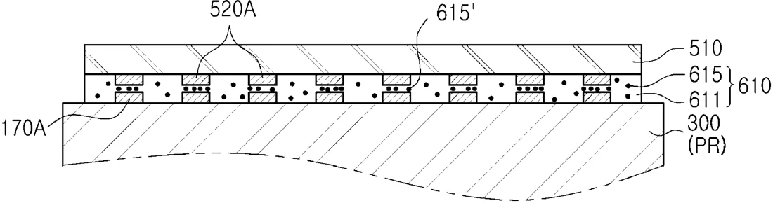
Samsung describes a display panel that uses LED cells for pixels and places connection points, or pads, on both the top and bottom edges. The design uses flexible circuit layers to connect these pads to the main processor, allowing signals to reach the screen from either side.
In the filing’s own words
A display apparatus may include a display panel including: a pixel array structure comprising LED cells configured as sub-pixels, the LED cells being in a display region of the display panel; and a driving circuit substrate on a lower surface of the pixel array structure and comprising a driving circuit configured to drive the LED cells. The display apparatus may further include: a plurality of upper pads on an upper surface of a pad region of the display panel, the pad region being on at least one side of the display region; a plurality of lower pads on a lower surface of the pad region; at least one through-via penetrating the driving circuit substrate and connecting the plurality of lower pads to the driving circuit; an upper flexible circuit layer connecting the plurality of upper pads; and a lower flexible circuit layer connecting the plurality of lower pads.
What exactly they claim (claim 1)
1. A display apparatus comprising: a display panel comprising: a pixel array structure comprising LED cells configured as sub-pixels, the LED cells being in a display region of the display panel; and a driving circuit substrate on a lower surface of the pixel array structure and comprising a driving circuit configured to drive the LED cells; a plurality of upper pads on an upper surface of a pad region of the display panel, the pad region being on at least one side of the display region; a plurality of lower pads on a lower surface of the pad region; at least one through-via penetrating the driving circuit substrate and connecting the plurality of lower pads to the driving circuit; a display processor configured to process image information and transmit an image signal to the driving circuit; an upper flexible circuit layer connecting the display processor and the plurality of upper pads; and a lower flexible circuit layer connecting the display processor and the plurality of lower pads.
Facts
- Company
- Samsung (SAMSUNG ELECTRONICS CO., LTD.)
- Official title
- DISPLAY APPARATUS INCLUDING DISPLAY PANEL WITH PAD REGIONS
- Publication number
- US20260324159A1
- Application number
- 19572097
- Filed
- Mar 19, 2026
- Published
- Oct 15, 2026
- Inventors
- 3
- Claims
- 20
Classified under
H10H 29/49 Electricity & electronicsH10H 29/32 Electricity & electronicsMore from Samsung in Chips & hardware
- Samsung patents chip that combines camera and screen Oct 13, 2026
- Samsung patents faster chip testing using machine learning Sep 1, 2026
- Samsung patents radar method to pinpoint target direction more accurately Sep 1, 2026
- Samsung patents memory chip that searches data by content, not address Sep 1, 2026
- Samsung patents chip design that skips empty data to speed up AI Sep 1, 2026
Summaries are simplified from the filing’s own abstract and first claim. A patent filing is not a product announcement.
Patent data and drawings: U.S. Patent and Trademark Office (USPTO). Nebula is not affiliated with or endorsed by the USPTO.