Samsung patents chip method using backside wiring to save space
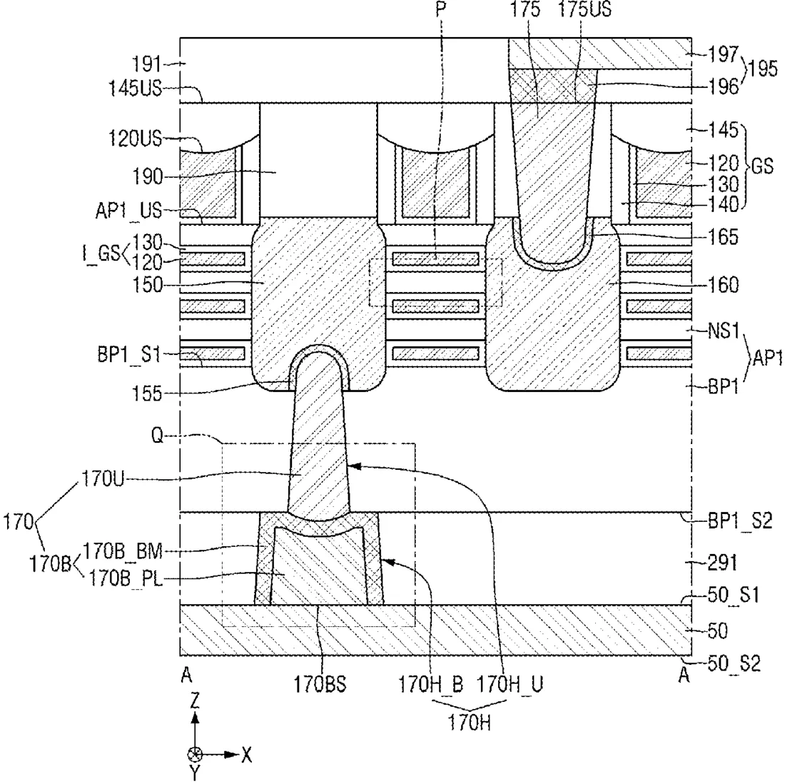
Samsung describes a way to build computer chips by adding electrical connections on the back of the silicon wafer. The process involves removing the original base and attaching new wiring lines to the back of the chip's internal components.
In the filing’s own words
A method for manufacturing a semiconductor device may include forming a first source/drain pattern on a substrate; forming a frontside wiring line on the first source/drain pattern; after removing the substrate, forming a backside interlayer insulating film on the first source/drain pattern, wherein the first source/drain pattern is disposed between the backside interlayer insulating film and the frontside wiring line; forming a contact silicide film connected to the first source/drain pattern; forming an upper contact pattern having a single conductive film structure and contacting the contact silicide film; forming a lower contact pattern connected to the upper contact pattern in the backside interlayer insulating film to form a backside source/drain contact including the upper contact pattern and the lower contact pattern; and forming a backside wiring line on the backside source/drain contact.
What exactly they claim (claim 1)
1. A method for manufacturing a semiconductor device, comprising: forming a first source/drain pattern on a substrate; forming a frontside wiring line on the first source/drain pattern; after removing the substrate, forming a backside interlayer insulating film on the first source/drain pattern, wherein the first source/drain pattern is disposed between the backside interlayer insulating film and the frontside wiring line; forming a contact silicide film connected to the first source/drain pattern; forming an upper contact pattern having a single conductive film structure and contacting the contact silicide film; forming a lower contact pattern connected to the upper contact pattern in the backside interlayer insulating film to form a backside source/drain contact including the upper contact pattern and the lower contact pattern; and forming a backside wiring line on the backside source/drain contact.
Facts
- Company
- Samsung (Samsung Electronics Co., Ltd.)
- Official title
- SEMICONDUCTOR DEVICE
- Publication number
- US20260323995A1
- Application number
- 19722099
- Filed
- Jun 26, 2026
- Published
- Oct 15, 2026
- Inventors
- 5
- Claims
- 20
Classified under
H10D 30/6729 Electricity & electronicsH10D 30/014 Electricity & electronicsH10D 30/43 Electricity & electronicsH10D 30/6735 Electricity & electronicsH10D 30/6757 Electricity & electronicsH10D 62/121 Electricity & electronicsMore from Samsung in Chips & hardware
- Samsung patents chip that combines camera and screen Oct 13, 2026
- Samsung patents faster chip testing using machine learning Sep 1, 2026
- Samsung patents radar method to pinpoint target direction more accurately Sep 1, 2026
- Samsung patents memory chip that searches data by content, not address Sep 1, 2026
- Samsung patents chip design that skips empty data to speed up AI Sep 1, 2026
Summaries are simplified from the filing’s own abstract and first claim. A patent filing is not a product announcement.
Patent data and drawings: U.S. Patent and Trademark Office (USPTO). Nebula is not affiliated with or endorsed by the USPTO.