Samsung patents chip layout with flat top surfaces for better manufacturing
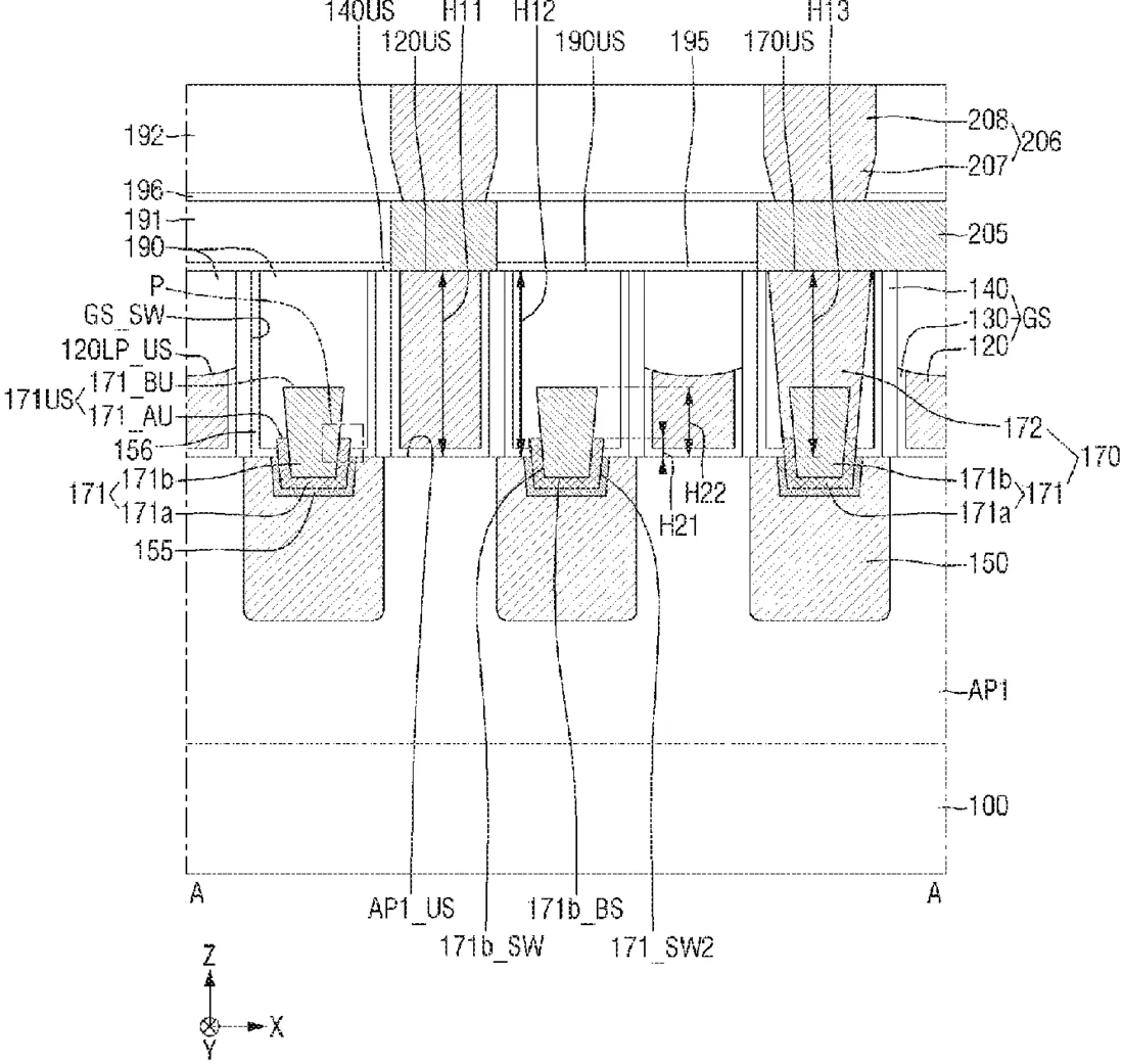
Samsung has filed a patent for a semiconductor design where the top of the gate electrode and the source/drain contact are at the same height. This flat alignment involves stacking a lower and upper contact layer to connect the chip's components.
In the filing’s own words
The semiconductor device including an active pattern on a substrate and extending in a first direction, a gate structure on the active pattern, including a gate electrode extending in a second direction different from the first direction, a source/drain pattern on at least one side of the gate structure, and a source/drain contact on the source/drain pattern and connected to the source/drain pattern, wherein with respect to an upper surface of the active pattern, a height of an upper surface of the gate electrode is same as a height of an upper surface of the source/drain contact, and the source/drain contact comprises a lower source/drain contact and an upper source/drain contact on the lower source/drain contact, may be provided.
What exactly they claim (claim 1)
1. A semiconductor device comprising: sheet patterns arranged in a first direction; a gate electrode surrounding a perimeter of each of the sheet patterns and extending in a second direction different from the first direction; a source/drain pattern connected to each of the sheet patterns; and a source/drain contact disposed on the source/drain pattern and connected to the source/drain pattern, wherein the sheet patterns comprise an uppermost sheet pattern, with respect to an upper surface of the uppermost sheet pattern, a height of an upper surface of the gate electrode is same as a height of an upper surface of the source/drain contact, and the source/drain contact comprises a lower source/drain contact and an upper source/drain contact on the lower source/drain contact.
Facts
- Company
- Samsung (Samsung Electronics Co., Ltd.)
- Official title
- SEMICONDUCTOR DEVICE AND METHOD FOR FABRICATING THE SAME
- Publication number
- US20260323986A1
- Application number
- 19717254
- Filed
- Jun 23, 2026
- Published
- Oct 15, 2026
- Inventors
- 4
- Claims
- 20
Classified under
H10D 30/6219 Electricity & electronicsH10D 30/503 Electricity & electronicsH10D 30/506 Electricity & electronicsH10D 30/6211 Electricity & electronicsH10D 62/121 Electricity & electronicsH10D 64/256 Electricity & electronicsMore from Samsung in Chips & hardware
- Samsung patents chip that combines camera and screen Oct 13, 2026
- Samsung patents faster chip testing using machine learning Sep 1, 2026
- Samsung patents radar method to pinpoint target direction more accurately Sep 1, 2026
- Samsung patents memory chip that searches data by content, not address Sep 1, 2026
- Samsung patents chip design that skips empty data to speed up AI Sep 1, 2026
Summaries are simplified from the filing’s own abstract and first claim. A patent filing is not a product announcement.
Patent data and drawings: U.S. Patent and Trademark Office (USPTO). Nebula is not affiliated with or endorsed by the USPTO.