Samsung patents chip design that turns wiring space into capacitors
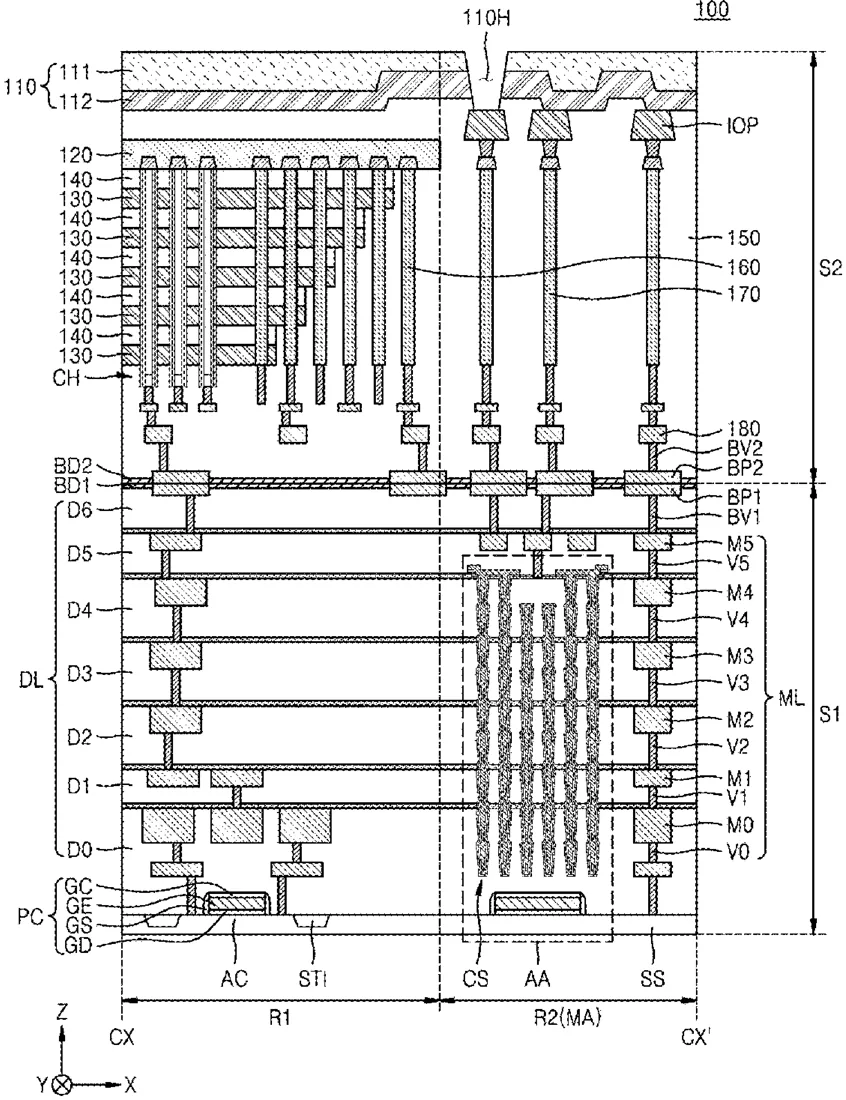
Samsung describes a semiconductor device where part of the standard wiring layers in the peripheral circuit area is replaced by a capacitor structure. This design uses a recessed area within the insulating layers to form the capacitor, allowing for a larger storage area without expanding the overall chip footprint.
In the filing’s own words
In the semiconductor device according to the inventive concept, part of a multi-layer wiring structure located in a wiring region of a peripheral circuit structure may be replaced by a replacement process to form a capacitor structure, and thus, there is the effect of improving electrical characteristics and reliability due to an increase in the area of the capacitor structure.
What exactly they claim (claim 1)
1. A semiconductor device comprising: a peripheral circuit structure comprising a substrate having an active region defined by a device isolation region, a peripheral circuit device on the active region, a multi-layer wiring structure connected to the peripheral circuit device, a multi-layer insulating structure surrounding the multi-layer wiring structure, a capacitor structure spaced apart from the multi-layer wiring structure in a horizontal direction and at least partially extending through the multi-layer insulating structure, and first bonding pads connected to the multi-layer wiring structure and the capacitor structure; and a memory cell structure comprising a passivation layer having a cell region and a pad region, gate electrodes stacked in the cell region and spaced apart from each other in a vertical direction, a channel structure extending through the gate electrodes, an input/output pad located in the pad region, a cover insulating layer covering the cell region and the pad region, a through-plug extending through the cover insulating layer in the pad region and connected to the input/output pad, a cell wiring structure connected to the channel structure and the through-plug, and second bonding pads connected to the cell wiring structure, wherein the capacitor structure comprises a first electrode layer conformally formed on an inner wall of a recess region at least partially extending through the multi-layer insulating structure, a capacitor dielectric layer conformally formed on an inner wall of the first electrode layer, and a second electrode layer in contact with an inner wall of the capacitor dielectric layer and filling the recess region, and at least a part of a first routing via, which is in contact with an upper surface of the first electrode layer, is positioned at substantially a same vertical level as at least a part of a second routing via in contact with an upper surface of the second electrode layer.
Facts
- Company
- Samsung (SAMSUNG ELECTRONICS CO., LTD.)
- Official title
- SEMICONDUCTOR DEVICE AND DATA STORAGE SYSTEM INCLUDING THE SAME
- Publication number
- US20260323950A1
- Application number
- 19573163
- Filed
- Mar 20, 2026
- Published
- Oct 15, 2026
- Inventors
- 5
- Claims
- 20
Classified under
H10B 43/40 Electricity & electronicsH10B 41/27 Electricity & electronicsH10B 41/35 Electricity & electronicsH10B 41/41 Electricity & electronicsH10B 43/27 Electricity & electronicsH10B 43/35 Electricity & electronicsMore from Samsung in Chips & hardware
- Samsung patents chip that combines camera and screen Oct 13, 2026
- Samsung patents faster chip testing using machine learning Sep 1, 2026
- Samsung patents radar method to pinpoint target direction more accurately Sep 1, 2026
- Samsung patents memory chip that searches data by content, not address Sep 1, 2026
- Samsung patents chip design that skips empty data to speed up AI Sep 1, 2026
Summaries are simplified from the filing’s own abstract and first claim. A patent filing is not a product announcement.
Patent data and drawings: U.S. Patent and Trademark Office (USPTO). Nebula is not affiliated with or endorsed by the USPTO.