Samsung patents plasma tool that tunes gas flow for chip making
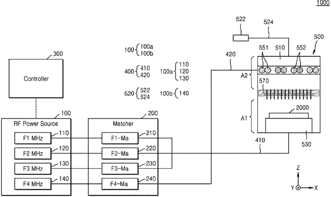
Samsung has filed a patent for a machine used to build computer chips that uses two separate areas to control plasma gas. The system adjusts electrical signals in specific zones to manage how the gas interacts with the silicon wafer during manufacturing.
In the filing’s own words
A plasma processing apparatus includes: a plasma chamber including a first area and a second area; a first radio frequency (RF) power source transmitting pieces of first RF power to the first area; a second RF power source transmitting second RF power to the second area; a controller configured to control the first RF power source and the second RF power source; and a first coil and a second coil arranged in the second area, wherein the controller spatially controls plasma in the first and second areas by controlling a signal of a current applied to the first coil and a signal of a current applied to the second coil, and temporally controls the plasma in the first and second areas by controlling a signal of the first RF power transmitted from the first RF power source and a signal of the second RF power transmitted from the second RF power source.
What exactly they claim (claim 1)
1. A method of manufacturing a semiconductor device, the method comprising: loading a wafer onto an electrostatic chuck inside a plasma chamber comprising a first area and a second area, wherein a first coil and a second coil, which are spatially separated from each other, are arranged in the second area; injecting a process gas into the plasma chamber; generating plasma by supplying a second radio frequency (RF) power to the second area of the plasma chamber; processing the wafer by supplying pieces of a first RF power to the first area of the plasma chamber; and unloading the wafer from the electrostatic chuck, wherein a signal of a current applied to the first coil and a signal of a current applied to the second coil are controlled such that the plasma in the first area or the second area is spatially controlled, and wherein changing an intensity of a current applied to a first coil and an intensity of a current applied to a second coil according to a composition ratio of the process gas in the first area.
Facts
- Company
- Samsung (SAMSUNG ELECTRONICS CO., LTD.)
- Official title
- PLASMA PROCESSING APPARATUS AND METHOD OF MANUFACTURING SEMICONDUCTOR DEVICE BY USING SAME
- Publication number
- US20260321543A1
- Application number
- 19462504
- Filed
- Jan 28, 2026
- Published
- Oct 15, 2026
- Inventors
- 5
- Claims
- 20
Classified under
H01J 37/32183 Electricity & electronicsH01J 37/32642 Electricity & electronicsH01J 37/32715 Electricity & electronicsH01J 2237/2007 Electricity & electronicsH01J 2237/334 Electricity & electronicsMore from Samsung in Chips & hardware
- Samsung patents chip that combines camera and screen Oct 13, 2026
- Samsung patents faster chip testing using machine learning Sep 1, 2026
- Samsung patents radar method to pinpoint target direction more accurately Sep 1, 2026
- Samsung patents memory chip that searches data by content, not address Sep 1, 2026
- Samsung patents chip design that skips empty data to speed up AI Sep 1, 2026
Summaries are simplified from the filing’s own abstract and first claim. A patent filing is not a product announcement.
Patent data and drawings: U.S. Patent and Trademark Office (USPTO). Nebula is not affiliated with or endorsed by the USPTO.