Samsung patents flash memory tweak to speed up data writing
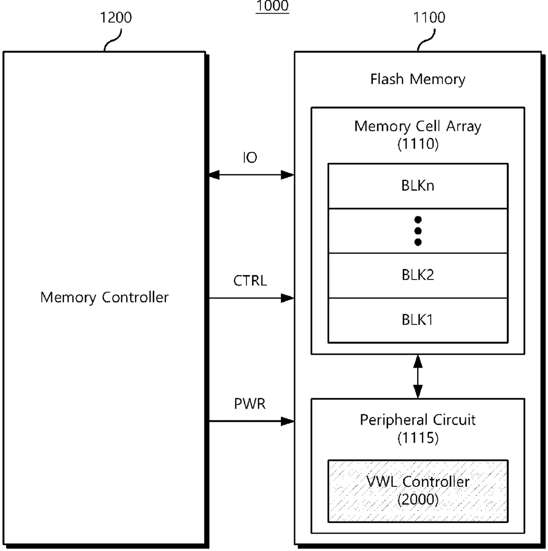
This filing describes a method for flash memory to reduce the time it takes to ramp up voltage when writing data. It adjusts the voltage levels applied to neighboring memory cells during the recovery phase after a write check to prepare for the next write cycle more quickly.
In the filing’s own words
The present disclosure provides methods and apparatuses for reducing a program voltage rising time. In some embodiments, a flash memory includes a memory cell array including a plurality of memory cells, a target voltage generator configured to adjust a target voltage level of a word line recovery voltage provided to the plurality of memory cells, and a word line voltage controller configured to provide recovery control signals for controlling the target voltage level of the word line recovery voltage. The target voltage generator is further configured to adjust the word line recovery voltage provided to a selected word line to the target voltage level, based on the recovery control signals provided during a word line recovery operation following a program verify operation, and to reduce a program voltage rising time in a program execution operation period of a next program loop by adjusting the target voltage level.
What exactly they claim (claim 1)
1. A flash memory, comprising: a memory cell array comprising a plurality of memory cells; a target voltage generator configured to adjust a target voltage level of a word line recovery voltage provided to the plurality of memory cells; and a word line voltage controller configured to provide recovery control signals for controlling the target voltage level of the word line recovery voltage, wherein the target voltage generator is further configured to: adjust the word line recovery voltage provided to a selected word line to the target voltage level based on the recovery control signals provided during a word line recovery operation following a program verify operation; and provide, during a program execution operation period of a next program loop, at least one of a first voltage and a first supply time of at least one pass voltage to word lines adjacent to the selected word line and at least one of a second voltage and a second supply time of at least another pass voltage to remaining unselected word lines, the first voltage being different from the second voltage, and the first supply time being different from the second supply time.
Facts
- Company
- Samsung (SAMSUNG ELECTRONICS CO., LTD.)
- Official title
- FLASH MEMORY REDUCING PROGRAM RISING TIME AND PROGRAM METHOD THEREOF
- Publication number
- US20260321325A1
- Application number
- 19720128
- Filed
- Jun 25, 2026
- Published
- Oct 15, 2026
- Inventors
- 3
- Claims
- 20
Classified under
G11C 16/3459 Physics & computingG11C 5/063 Physics & computingG11C 5/147 Physics & computingG11C 8/08 Physics & computingG11C 11/4074 Physics & computingG11C 16/0483 Physics & computingMore from Samsung in Chips & hardware
- Samsung patents chip that combines camera and screen Oct 13, 2026
- Samsung patents faster chip testing using machine learning Sep 1, 2026
- Samsung patents radar method to pinpoint target direction more accurately Sep 1, 2026
- Samsung patents memory chip that searches data by content, not address Sep 1, 2026
- Samsung patents chip design that skips empty data to speed up AI Sep 1, 2026
Summaries are simplified from the filing’s own abstract and first claim. A patent filing is not a product announcement.
Patent data and drawings: U.S. Patent and Trademark Office (USPTO). Nebula is not affiliated with or endorsed by the USPTO.