Samsung patents new way to manage NAND memory space
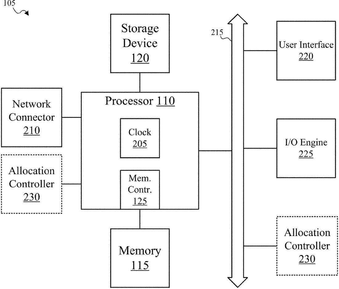
Samsung has filed a patent for a system that manages NAND flash memory by creating separate translation layers for different sections of the storage. The method uses a list of available space to assign these sections and tracks them in an allocation list.
In the filing’s own words
Provided are systems, methods, and apparatuses for byte-addressable NAND memory. In one or more examples, the systems, devices, and methods include generating a first flash translation layer for a first allocation of a memory device; generating a second flash translation layer for a second allocation of the memory device, the first allocation and the second allocation being based on a pool of allocation space indicated in a freelist; and adding at least one of the first allocation or the second allocation to an allocation list based on generating at least one of the first flash translation layer or the second flash translation layer.
What exactly they claim (claim 1)
1. A method comprising: generating a first flash translation layer for a first allocation of a memory device; generating a second flash translation layer for a second allocation of the memory device, the first allocation and the second allocation being based on a pool of allocation space indicated in a freelist; and adding at least one of the first allocation or the second allocation to an allocation list based on generating at least one of the first flash translation layer or the second flash translation layer.
Facts
- Company
- Samsung (Samsung Electronics Co., Ltd.)
- Official title
- SYSTEMS AND METHODS OF BYTE-ADDRESSABLE NAND MEMORY
- Publication number
- US20260319679A1
- Application number
- 19402976
- Filed
- Nov 26, 2025
- Published
- Oct 15, 2026
- Inventors
- 3
- Claims
- 20
Classified under
G06F 3/0631 Physics & computingG06F 3/0608 Physics & computingG06F 3/0679 Physics & computingMore from Samsung in Chips & hardware
- Samsung patents chip that combines camera and screen Oct 13, 2026
- Samsung patents faster chip testing using machine learning Sep 1, 2026
- Samsung patents radar method to pinpoint target direction more accurately Sep 1, 2026
- Samsung patents memory chip that searches data by content, not address Sep 1, 2026
- Samsung patents chip design that skips empty data to speed up AI Sep 1, 2026
Summaries are simplified from the filing’s own abstract and first claim. A patent filing is not a product announcement.
Patent data and drawings: U.S. Patent and Trademark Office (USPTO). Nebula is not affiliated with or endorsed by the USPTO.