Samsung patents chip package with built-in light guide for data
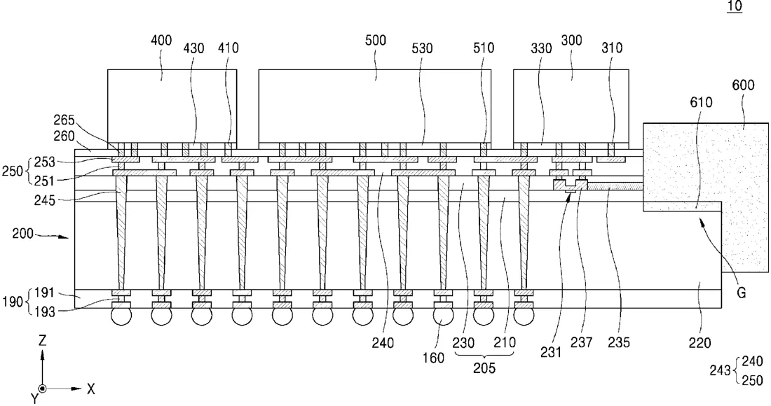
Samsung describes a semiconductor package that combines standard electronic chips with a light guide, or waveguide, inside the base material. The design includes a specific groove on the top surface where an optical fiber plugs in to send light signals directly to the chip's internal components.
In the filing’s own words
A semiconductor package includes a body having an upper surface and a lower surface and including a groove extending downward from the upper surface of the body in a vertical direction, an oxide layer on the body, including therein a waveguide and an optical component connected to the waveguide, and not overlapping the groove of the body in the vertical direction, an upper wiring layer on the oxide layer and including an upper wiring pattern and an upper wiring insulating layer, a through-electrode connected to the upper wiring pattern and passing through the body and the oxide layer in the vertical direction, a bonding pad, a bonding insulating layer, an electronic integrated circuit chip on the bonding pad and the bonding insulating layer, and an optical fiber mounted in the groove via a protrusion and in contact with the upper wiring layer in a lateral direction.
What exactly they claim (claim 1)
1. A semiconductor package comprising: a body having an upper surface and a lower surface, wherein the body comprises a groove extending downward from the upper surface of the body in a vertical direction; an oxide layer on the body; a waveguide and an optical component connected to the waveguide, wherein the waveguide and the optical component are in the oxide layer, and wherein the waveguide and the optical component are spaced apart from the groove of the body in a horizontal direction; an upper wiring layer on the oxide layer, wherein the upper wiring layer comprises an upper wiring pattern and an upper wiring insulating layer surrounding the upper wiring pattern; a through-electrode electrically connected to the upper wiring pattern, wherein the through-electrode extends in the body and the oxide layer in the vertical direction; a bonding pad on the upper wiring layer; a bonding insulating layer surrounding a side surface of the bonding pad; an electronic integrated circuit (EIC) chip on the bonding pad and the bonding insulating layer; and an optical fiber mounted on the groove, wherein the optical fiber comprises a protrusion extending into the groove, and wherein the optical fiber is in contact with the upper wiring layer in the horizontal direction.
Facts
- Company
- Samsung (Samsung Electronics Co., Ltd.)
- Official title
- SEMICONDUCTOR PACKAGE
- Publication number
- US20260319169A1
- Application number
- 19467365
- Filed
- Feb 2, 2026
- Published
- Oct 15, 2026
- Inventors
- 1
- Claims
- 20
Classified under
G02B 6/12004 Physics & computingG02B 6/12002 Physics & computingG02B 6/122 Physics & computingH10B 80/00 Electricity & electronicsH10D 80/30 Electricity & electronicsH10W 20/222 Electricity & electronicsMore from Samsung in Chips & hardware
- Samsung patents chip that combines camera and screen Oct 13, 2026
- Samsung patents faster chip testing using machine learning Sep 1, 2026
- Samsung patents radar method to pinpoint target direction more accurately Sep 1, 2026
- Samsung patents memory chip that searches data by content, not address Sep 1, 2026
- Samsung patents chip design that skips empty data to speed up AI Sep 1, 2026
Summaries are simplified from the filing’s own abstract and first claim. A patent filing is not a product announcement.
Patent data and drawings: U.S. Patent and Trademark Office (USPTO). Nebula is not affiliated with or endorsed by the USPTO.