Samsung patents curved pads for stacking semiconductor chips
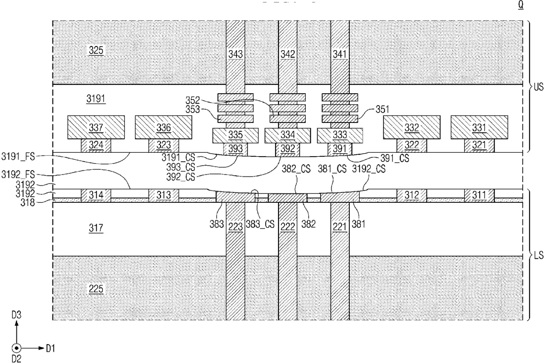
Samsung describes a method for building semiconductor packages by stacking two chip structures together. The design uses curved metal pads on the bottom of the top chip and the top of the bottom chip to connect them. This allows the two layers to bond securely using curved surfaces rather than flat ones.
In the filing’s own words
A method for fabricating a semiconductor package includes forming a lower structure including a first semiconductor substrate and a lower through structure penetrating the first semiconductor substrate, forming a lower curved pad on the lower through structure, forming an upper structure including a second semiconductor substrate and an upper through structure penetrating the second semiconductor substrate, forming an upper curved pad connected to the upper through structure, and bonding the lower structure and the upper structure such that the upper curved pad is positioned on the lower curved pad, where a top surface of the lower curved pad includes a curved surface and a bottom surface of the upper curved pad includes a curved surface.
What exactly they claim (claim 1)
1. A method for fabricating a semiconductor package, comprising: forming a lower structure comprising a first semiconductor substrate and a lower through structure penetrating the first semiconductor substrate; forming a lower curved pad on the lower through structure; forming an upper structure comprising a second semiconductor substrate and an upper through structure penetrating the second semiconductor substrate; forming an upper curved pad connected to the upper through structure; and bonding the lower structure and the upper structure such that the upper curved pad is positioned on the lower curved pad, wherein a top surface of the lower curved pad comprises a curved surface, and wherein a bottom surface of the upper curved pad comprises a curved surface.
Facts
- Company
- Samsung (SAMSUNG ELECTRONICS CO., LTD.)
- Official title
- SEMICONDUCTOR PACKAGE
- Publication number
- US20260314497A1
- Application number
- 19712959
- Filed
- Jun 18, 2026
- Published
- Oct 8, 2026
- Inventors
- 1
- Claims
- 20
Classified under
H10W 90/00 Electricity & electronicsH10W 80/00 Electricity & electronicsH10W 72/01953 Electricity & electronicsH10W 72/90 Electricity & electronicsH10W 72/923 Electricity & electronicsH10W 72/926 Electricity & electronicsMore from Samsung in Chips & hardware
- Samsung patents chip that combines camera and screen Oct 13, 2026
- Samsung patents faster chip testing using machine learning Sep 1, 2026
- Samsung patents radar method to pinpoint target direction more accurately Sep 1, 2026
- Samsung patents memory chip that searches data by content, not address Sep 1, 2026
- Samsung patents chip design that skips empty data to speed up AI Sep 1, 2026
Summaries are simplified from the filing’s own abstract and first claim. A patent filing is not a product announcement.
Patent data and drawings: U.S. Patent and Trademark Office (USPTO). Nebula is not affiliated with or endorsed by the USPTO.