Samsung patents chip package with antenna built into side wiring
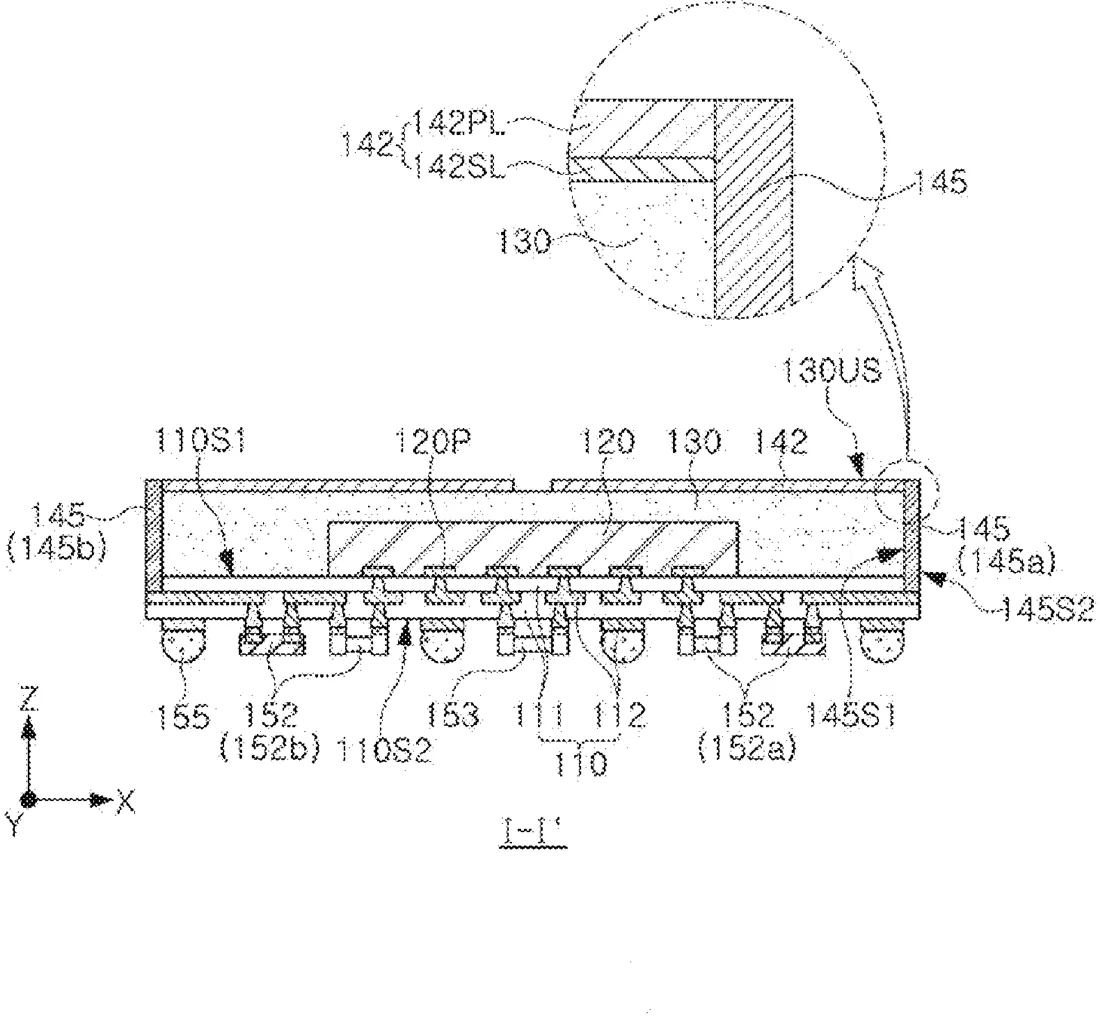
Samsung describes a method for making a semiconductor package where an antenna is placed on top of the chip's protective coating. The company explains how to create a side connection by drilling a hole through the coating, filling it with metal, and cutting the package to leave a metal line on the side that links the antenna to the chip.
In the filing’s own words
Provided is a semiconductor package including a redistribution structure including first surface and a second surface opposite to each other, the redistribution structure including a redistribution layer, a semiconductor chip on the first surface of the redistribution structure, the semiconductor chip being electrically connected to the redistribution layer, an encapsulant on the semiconductor chip, at least one antenna pattern on the encapsulant, a side wiring line extending along a surface of the encapsulant from one end of the antenna pattern to the redistribution layer, and electronic devices on the second surface of the redistribution structure, the electronic devices being electrically connected to the redistribution layer, wherein the semiconductor chip and the antenna pattern are configured to transmit and receive a signal to and from each other through the electronic devices.
What exactly they claim (claim 1)
1. A method for manufacturing a semiconductor package comprising: forming a molded structure having a plurality of unit packages defined by sawing lines, wherein each of the plurality of unit packages includes a redistribution structure, a semiconductor chip on the redistribution structure, and an encapsulant covering the semiconductor chip; forming a plurality of antenna patterns on the molded structure, wherein at least one antenna pattern is disposed on an upper surface of the encapsulant of each of the plurality of unit packages; forming a plurality of holes penetrating through the encapsulant in a vertical direction and crossing the sawing lines in a horizontal direction, wherein each of the plurality of holes exposes at least one end of the at least one antenna pattern in the horizontal direction; forming a conductive material layer in each of the plurality of holes, wherein the conductive material layer is in contact with the at least one end of the at least one antenna pattern; and separating the molded structure into the plurality of unit packages by cutting the conductive material layer, the encapsulant, and the redistribution structure along the sawing lines, wherein each of the plurality of unit packages has a trench formed by cutting one of the plurality of holes in the vertical direction, and a side wiring line formed by cutting the conductive material layer in the one of the plurality of holes in the vertical direction.
Facts
- Company
- Samsung (SAMSUNG ELECTRONICS CO., LTD.)
- Official title
- SEMICONDUCTOR PACKAGE AND METHOD OF MANUFACTURING SEMICONDUCTOR PACKAGE
- Publication number
- US20260314417A1
- Application number
- 19461207
- Filed
- Jan 27, 2026
- Published
- Oct 8, 2026
- Inventors
- 6
- Claims
- 20
Classified under
H10W 42/00 Electricity & electronicsH01Q 9/0407 Electricity & electronicsH10W 70/685 Electricity & electronicsH10W 74/117 Electricity & electronicsH10W 90/00 Electricity & electronicsMore from Samsung in Chips & hardware
- Samsung patents chip that combines camera and screen Oct 13, 2026
- Samsung patents faster chip testing using machine learning Sep 1, 2026
- Samsung patents radar method to pinpoint target direction more accurately Sep 1, 2026
- Samsung patents memory chip that searches data by content, not address Sep 1, 2026
- Samsung patents chip design that skips empty data to speed up AI Sep 1, 2026
Summaries are simplified from the filing’s own abstract and first claim. A patent filing is not a product announcement.
Patent data and drawings: U.S. Patent and Trademark Office (USPTO). Nebula is not affiliated with or endorsed by the USPTO.