Samsung patents chip design with curved layers to cut power waste
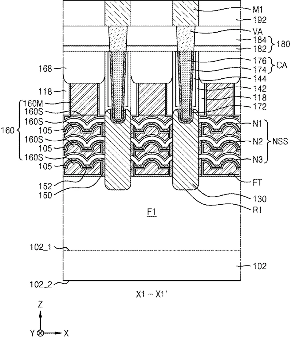
Samsung describes an integrated circuit where the channel layers, made of a material called transition metal dichalcogenide, are shaped with curved bumps instead of being flat. The design also leaves a specific gap between the gate and the source/drain area without filling it with insulating material to reduce unwanted electrical interference.
In the filing’s own words
Provided are an integrated circuit device and a method of manufacturing the same, wherein, in the integrated circuit device, a curved channel layer is arranged to improve electrical characteristics, and a gate insulating material is not formed in an inner spacer formed on sidewalls of a source/drain region, and thus parasitic capacitance is reduced.
What exactly they claim (claim 1)
1. An integrated circuit device comprising: an active region extending in a first horizontal direction on a substrate; a plurality of channel layers apart from each other on the active region in a vertical direction, and extending in the first horizontal direction; oxide layers under the plurality of channel layers, respectively; a gate line extending on the active region in a second horizontal direction crossing the first horizontal direction, and surrounding the plurality of channel layers and the oxide layers; a source/drain region on the active region and in contact with the plurality of channel layers; and an inner spacer, wherein the inner spacer comprises: one sidewall in contact with a sidewall of the source/drain region; another sidewall opposite the one sidewall and on a sidewall of the gate line; and an upper surface and a lower surface, each in contact with the plurality of channel layers, wherein the plurality of channel layers comprise a transition metal dichalcogenide (TMD) compound, and wherein each of the plurality of channel layers comprises a plurality of convex curved units in the vertical direction.
Facts
- Company
- Samsung (SAMSUNG ELECTRONICS CO., LTD.)
- Official title
- INTEGRATED CIRCUIT DEVICE
- Publication number
- US20260314048A1
- Application number
- 19337121
- Filed
- Sep 23, 2025
- Published
- Oct 8, 2026
- Inventors
- 4
- Claims
- 20
Classified under
H10D 84/832 Electricity & electronicsH10D 30/43 Electricity & electronicsH10D 30/481 Electricity & electronicsH10D 30/503 Electricity & electronicsH10D 62/102 Electricity & electronicsH10D 62/121 Electricity & electronicsMore from Samsung in Chips & hardware
- Samsung patents chip that combines camera and screen Oct 13, 2026
- Samsung patents faster chip testing using machine learning Sep 1, 2026
- Samsung patents radar method to pinpoint target direction more accurately Sep 1, 2026
- Samsung patents memory chip that searches data by content, not address Sep 1, 2026
- Samsung patents chip design that skips empty data to speed up AI Sep 1, 2026
Summaries are simplified from the filing’s own abstract and first claim. A patent filing is not a product announcement.
Patent data and drawings: U.S. Patent and Trademark Office (USPTO). Nebula is not affiliated with or endorsed by the USPTO.